While the Altera DE1 board has been a great development platform for the MiniSOC project, I don’t want the project to live on that board forever. I’ve bought a relatively cheap Cyclone 3 board from EBay featuring an EP3C25 FPGA (this is the same FPGA as appears in the Turbo Chameleon 64), which has a shade under 25,000 logic elements to play with. (The board in question can be found here: http://www.ebay.co.uk/itm/Cyclone-III-FPGA-EP3C25-board-/270910317225 – that version has only a single 8-bit wide SDRAM chip, but when I contacted the sellers they were extremely helpful, and added a second chip for just $5 extra.)
I have a rather nice small form factor case in which I’d like to install this project, but the case has a PC-style momentary push-button power switch, so I need some kind of latching power circuit.
The requirements for the circuit are:
- Must draw only negligible power in the “off” state.
- Must latch reasonably quickly, and not turn off again until the button is released and pressed again.
- If FPGA signal pins are used, must not allow voltage to reach them in the “off” state.
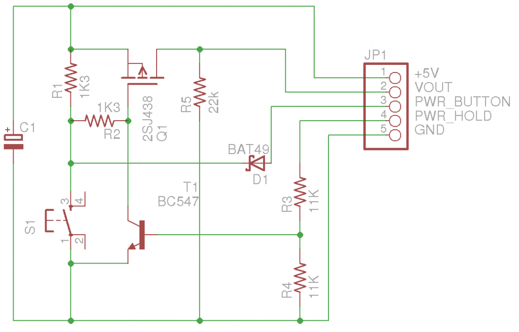
After studying a few similar circuits on the web, I decided to use a P-channel MOSFET and a BC547, with the base of the latter being driven by the FPGA.
The schematic of my current circuit is as follows:
A few explanatory notes:
- PWR_BUTTON and PWR_HOLD are signal pins on the FPGA. The FPGA is powered from VOUT.
- S1 triggers the MOSFET and allows power to flow to VOUT
- The FPGA fires up, and as soon as it’s configured, sets PWR_HOLD to a high output, causing the BC547 to keep the MOSFET open.
- The FPGA sets PWR_BUTTON to an input with weak pullup, allowing it to detect a second press of the button. D1 prevents +5V reaching the non-5v-tolerant FPGA pin, and also prevents any voltage reaching that pin while the FPGA is off. R2 prevents the action of the BC547 interfering with the button press detection.
- R5 is a load resister that just drains away any stray charge that’s left when the circuit powers off.
The button itself has to be debounced in the FPGA. The easiest way to do this is just to begin a delay any time the button line’s state changes, then sample it a second time when the delay’s elapsed, and compare.
The VHDL looks like this:
signal debounce_counter : unsigned(11 downto 0) := X"fff";
signal power_button_deb : std_logic;
signal power_button_deb1 : std_logic;
...
-- debounce the power switch
    process(clk)
    begin
        if rising_edge(clk) then
            if debounce_counter=X"000" then
                if power_button_deb1='1' and power_button='1' then    -- Is button stable?
                    power_button_deb<='1';
                elsif power_button_deb1='0' and power_button='0' then
                    power_button_deb<='0';
                else -- No? Start a delay...
                    debounce_counter<=X"FFF";
                end if;
                power_button_deb1 <= power_button;
            else
                debounce_counter<=debounce_counter-1;
            end if;
        end if;
    end process;


Thanks for all the step by step tutorials. It is a valuable resource.
There is a stack-up board for the Ep3C25 board with VGA, LED, LCD and SD connectors but some of the smd color resistors DAC for the VGA is wrongly routed.
Nothing too difficult to correct. FYI.
rgds
lak