
Part 14: Improving the SDRAM controller
One limitation of the MiniSOC project so far has been that only a very basic 16-bit 640×480@60Hz screenmode is supported. The reason for this is mainly RAM bandwidth, since the boards I’m targetting have single-data-rate SDRAM.
The SDRAM controller I’m using is derived from the one Tobias Gubener created for the TG68-based versions of the Minimig core. The original controller used 4-word bursts when reading from SDRAM, wrote in single words, and operated on a fixed 16-clock cycle, which had the advantage of guaranteeing a deterministic response time for the Amiga emulation.
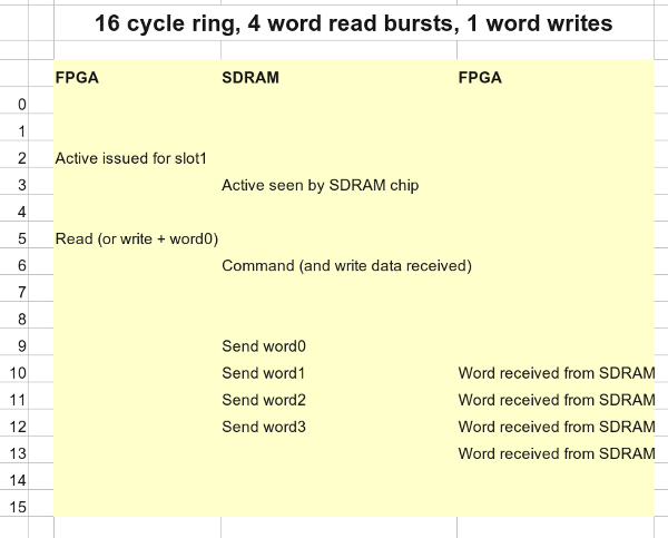
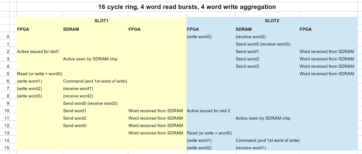
In the work I did improving the Minimig core, I extended this so that writes also operated in burst mode, and took advantage of bank interleaving to add a second access slot to the SDRAM controller – while maintaining the fixed 16-clock cycle. The sequence of events looks something like this:
While this allowed a significant speedup for the Minimig core, and allowed for a VGA framebuffer for the TG68MiniSOC project, resolution is limited by memory bandwidth; the standard 640x480x16@60Hz screenmode in 16-bit colour more or less saturates the first access slot, leaving the other free for the CPU (when bank interleaving allows.)
Recently, however, I’ve wanted to increase the screen resolution to 800×600 or above at 16-bit. The most popular 800x600x16 screenmode runs at 72Hz, and uses a pixel clock of 50Mhz (rather than the 25MHz pixel clock for 640×480@60Hz) which means I’ll need to double the RAM bandwidth in order to achieve this.
So how to approach this?
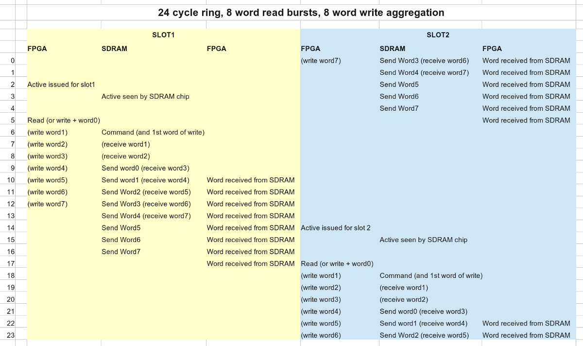
The first thing we can do is increase the burst length from 4 words to 8 words. Getting this working turned out to be more tedious work than I expected, because the controller itself is a bit of a tangle, and the increased burst length shook out a few bugs elsewhere in the project, but eventually I did get this working stably. It required a 24-cycle ring, though, rather than 16, which means the increase in bandwidth was only 50%, not 100%.
Nevertheless, after a complete re-architecting of the DMA cache, this was sufficient to implement something close to the standard 800x600x16@56Hz screenmode. This would normally require a 36MHz pixel clock, and the closest I could easily achieve was 33Mhz, but nonetheless my monitor displayed a picture, and the impact on Dhrystone score wasn’t huge, so I was happy.
I couldn’t help thinking that the quest for more bandwidth needn’t be in vain, however. If you’re just reading from SDRAM then using bank interleave tricks it’s possible to transfer data on every single clock, while my 24-cycle ring version of the controller has a theoretical maximum of 16 words per 24 cycle circuit.
Overlapping accesses to different banks is complicated by the 3-cycle CAS latency of the SDRAM, or more precisely by the fact that the latency only applies to reads, not writes. Ideally we want reads and writes to occupy the same “space” in the routine, so they can overlap more tightly. In actual operation, it turns out that the write cache doesn’t make a massive difference to the ultimate CPU speed, because generally the CPU can only write 2 words to the cache before the write has been serviced. Those two words are usually just a long-word (32-bit) write, aggregated into a pair of word writes, so reducing the size of the write cache to two words has only minimal impact on speed. What this buys us is the ability to delay writes so that they happen a few cycles later, and allowing us to “collapse” the 24-cycle ring into a 16-cycle ring, the same size as the original controller, but with double the bandwidth.
The final sequence of events looks like this:
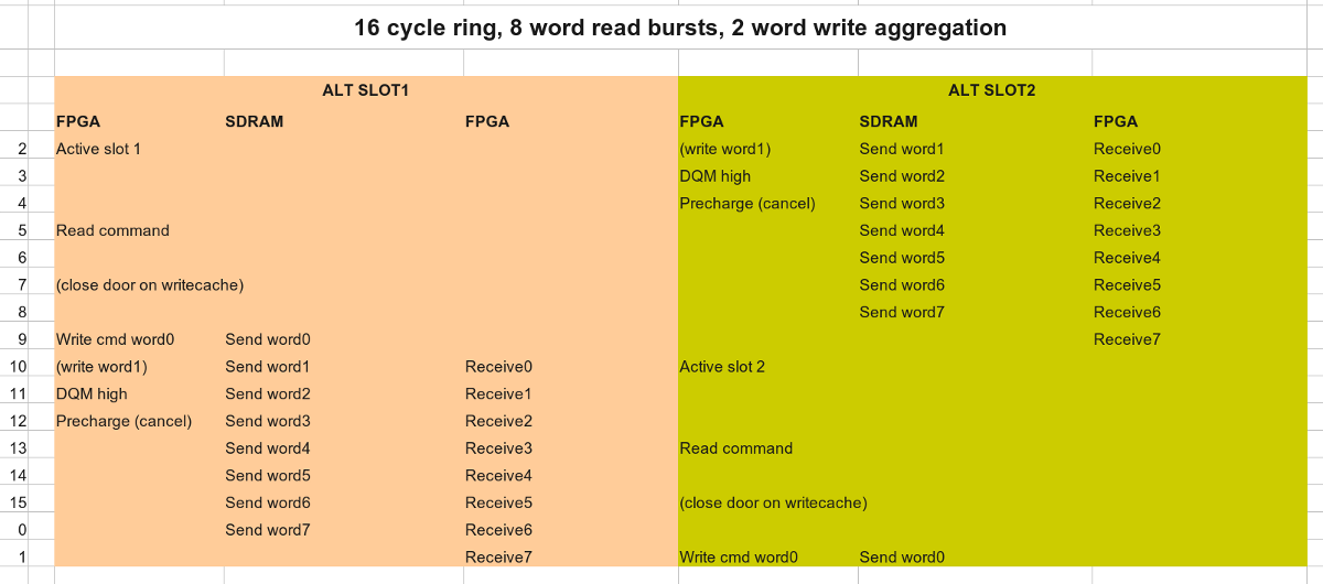
Using this version of the SDRAM controller, the TG68MiniSOC project is now capable of displaying an 800×600 16-bit framebuffer at 72Hz refresh rate.
As always, full source can be found on my GitHub page – tagged accordingly: https://github.com/robinsonb5/TG68_MiniSOC/releases/tag/20140505_Part14
If you want to try it out, build one of the project files in SOC/fpga/ then build Apps/Demo or Apps/Screenmodes
The S-record can either be updated over RS232, or copied to an SD card and booted from there. (rename it to “boot.sre”.)
In the main Demo app, the screenmode can be selected with F4-F9. Note that while the screenmode changes, the demo currently makes no effort to redraw what’s on screen to fit the new size, so it’ll look scrambled.
In the Screenmodes demo app, F1 – F5 selects screenmode, and the testcard will be redrawn to fit the new size.
Thanks a lot for this long writeup of the SDRAM controller !
Just one remark to the screen resolutions, I personally prefer to seen the color depth in a specification too, as it is really part of it, so:
640×480×16@60Hz screenmode, 800×600×16@72 seems better.
But as I said, personal preference 😉
GOOD JOB!
Good point – I’ve just updated the post accordingly. 🙂
Hi! I’m using a dram controller derived from one chip msx one. It uses follow 8 steps/cl3/burst 1 scheme:
Act Nop ReadA Nop Nop Dat Nop Nop
Why do you insert 2 nops between act and reada commands? Burst 4 can be completed in 12 steps. Tnx for Your tutorial.
Saverio
A quick look at a couple of datasheets tells me that the Active to Read/Write (RAS to CAS) delay is typically at least 18ns and sometimes over 20. If it’s 20 or less and you’re clocked at no more than 100Mhz then one nop is fine. Two nops allows the controller to work with slower parts, and be clocked up to 133Mhz or possibly even beyond for faster parts. (Though my cache wouldn’t be able to keep pace with that!)