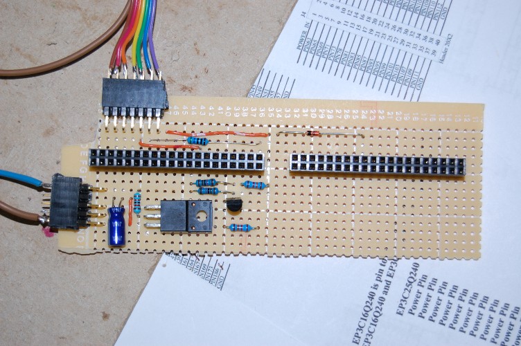
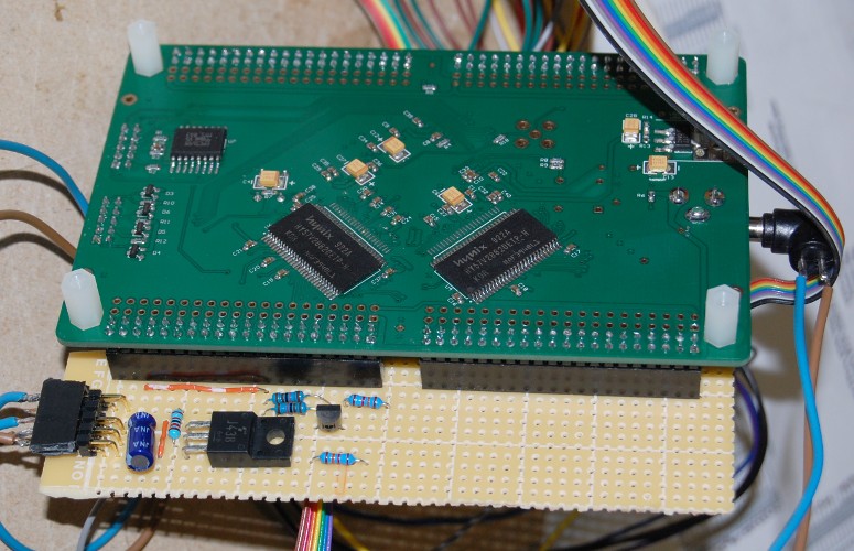
Having breadboarded the latching power circuit from my last post and found it works pretty well, I’ve made a more permanent version that plugs directly onto the headers on my Cyclone 3 board. While I’d normally build something like this on stripboard, it’s not really appropriate for this project because the pins on the 40-pin headers are only one row of holes apart. Therefore I’ve used matrix board this time around.
This is the case I plan to use to house this project. It’s the case from an old, dead Acer Aspire L320 – a nice looking machine that, unfortunately, seems to have insufficient chipset cooling, so tends to die a horrible death. Dead ones crop up on Ebay fairly frequently, and with a little bit of cleaning up and removing of label residue, they’re an ideal housing for a project like this one.
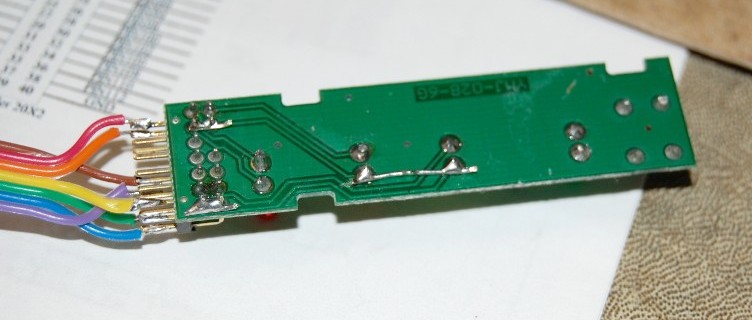
Behind the power button is a little circuit board with four LEDs (actually only three on mine, but space for a fourth) and the actual power button switch. I rewired this board slightly – removed the blue LEDs (*please* people, can we get over the blue LED thing now!) and replaced them with green, yellow, orange and red ones. I also wired the LED anodes in common, to keep the component count down. The common anode will be fed from 3.3v through a small resitor, then the four LEDs’ cathodes will be tied directly to FPGA pins. When the respective FPGA pin is low, the LED will light up.
The obvious problem with this arrangement is that when more than one LED is lit, the current will be shared between them, making them dimmer – to avoid this, I’ll use a pulse-width modulation system, giving each LED a 25% duty cycle, and alternating between them, so no two LEDs will be lit at the same time.
The VHDL code for this is as follows:
library ieee;
use ieee.std_logic_1164.all;
use ieee.std_logic_unsigned.all;
use IEEE.numeric_std.ALL;

entity statusleds_pwm is
    port(
        clk : in std_logic;
        leds_in : in std_logic_vector(3 downto 0);
        leds_out : out std_logic_vector(3 downto 0)
    );
end statusleds_pwm;

architecture rtl of statusleds_pwm is
    signal counter : unsigned(18 downto 0);
begin
    process(clk)
    begin
        if rising_edge(clk) then
            counter <= counter+1;
            if counter(16 downto 0)=X"0000"&"0" then
                leds_out<="1111";
                case counter(18 downto 17) is
                    when "00" =>
                        leds_out(0)<=not leds_in(0);
                    when "01" =>
                        leds_out(1)<=not leds_in(1);
                    when "10" =>
                        leds_out(2)<=not leds_in(2);
                    when "11" =>
                        leds_out(3)<=not leds_in(3);
                end case;
            end if;
        end if;
    end process;
end architecture;
As I mentioned in my previous post, the Cyclone 3 board I’m using has four general purpose IO headers, but two of these headers share FPGA pins with the RAM chips, so on a board like mine that’s populated with two RAM chips, there are only a handful of available IOs on headers J3 and J4. There are, however, enough to run my latching power circuit, the LEDs, and a couple left over which I’ll use for an RS232 port.
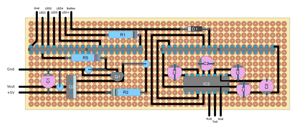
The following matrix board layout describes a board which connects directly to headers J3 and J4 on the FPGA board, leaving the IO-rich J1 and J2 free for A/V, SD Card and joystick interfaces.
I’m currently waiting for delivery of some MAX3232s (MAX232 variant that runs from 3.3v) – so that part of the board isn’t yet built – but the power aspect is built and working. 
(The above is not quite the final version – I moved one signal to a different IO pin, and added a small capacitor between LED+ and GND.)


