
Part 3: Clocking
The EMS11-BB21 board I received a few weeks ago has a Spartan 6 FPGA which the board provides with a 50MHz clock. In the examples so far I’ve used that clock directly – but FPGAs generally have the ability to be much more flexible where clocking’s concerned, and the Spartan 6 is no exception.
For the Altera versions of these projects, I’ve used a “Megafunction Wizard” to generate a component which configures one of the FPGA’s PLLs (Phase Lock Loop) to generate the clocks I need. These can take an input clock, generate a much faster clock, then divide that by a selectable divisor. So while you can’t get an arbitrary output frequency from a PLL, you can get close enough within reasonable limits for practical purposes.
Naturally I started looking for the Xilinx equivalent of the Megafunction Wizard in ISE, and didn’t have far to look. Simply go to Project -> New Source, and select “IP (Core generator and Architecture Wizard)”
Once you’ve picked a location and filename for the component, in the list of functions that appears unfold “FPGA Features and Design”, then “Clocking”, then “Clocking Wizard”. (If you’ve ticked the “Only IP compatible with chosen part” checkbox, then that will be the only entry under Clocking.”
Click through to the end of the Wizard, and wait – after a short pause the Clocking Wizard itself will appear.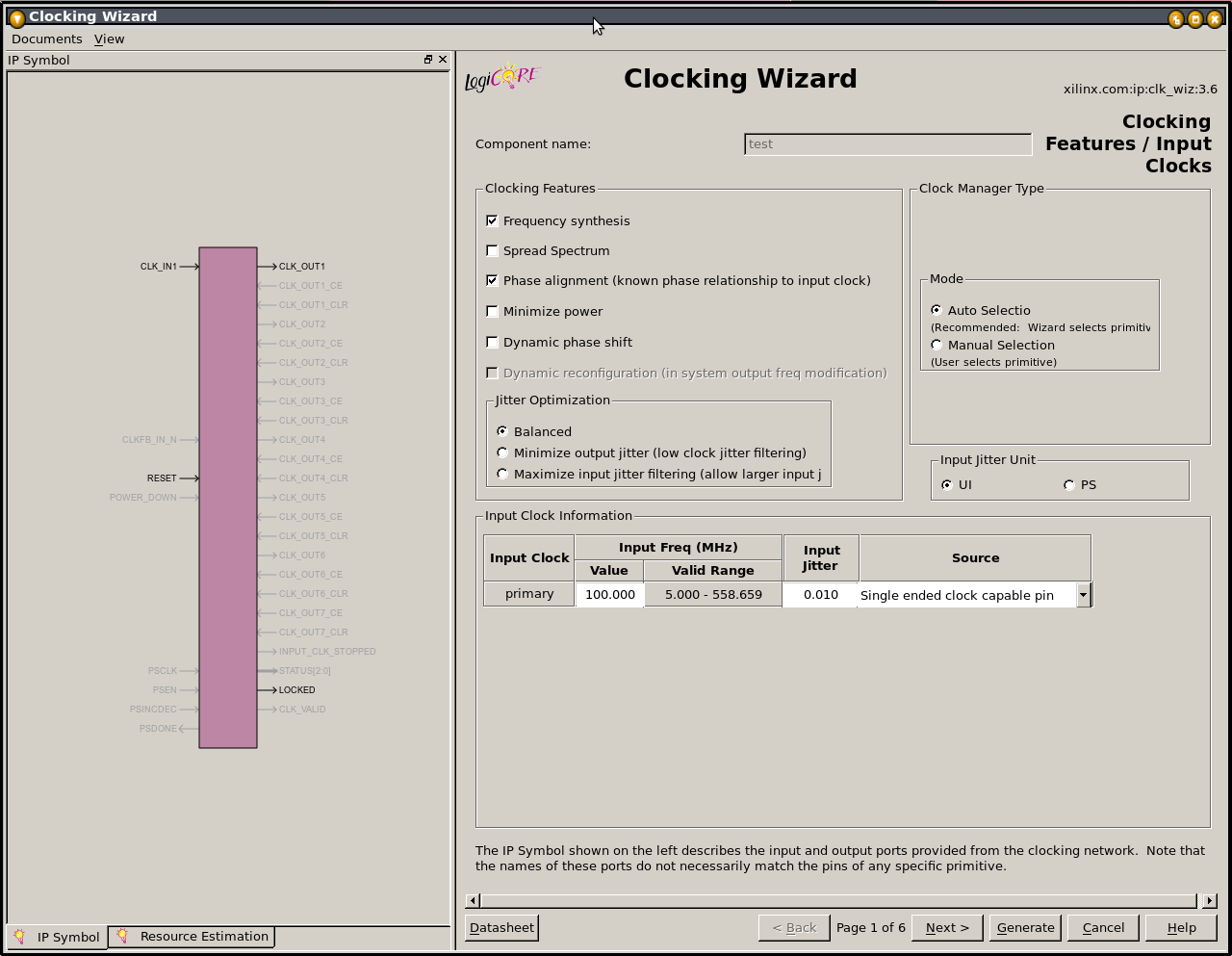
Our input clock frequency in this case is 50MHz, so we’d change the 100 that’s there by default. Since I don’t intend to use the 50MHz clock for anything other than running the clock generator, we can also uncheck “Phase alignment”. We’d leave that selected if we were going to run part of the design from the 50MHz clock and needed to transfer data between the clock domains. Having made those two changes, we can click “Next”.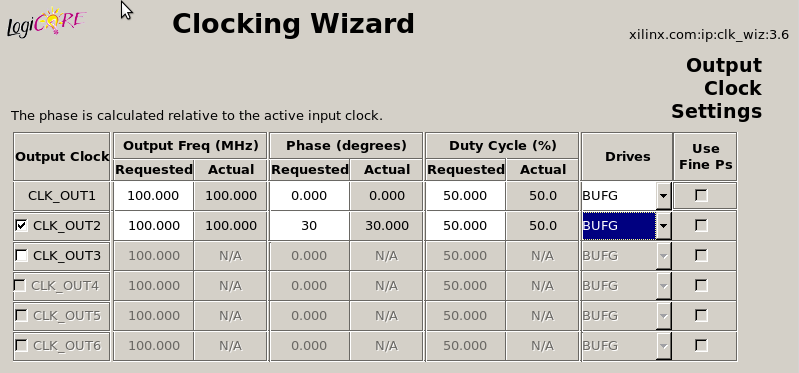
Here we can choose our output clocks. They don’t have to be the same frequency, but not all combinations of frequencies are possible – the “actual” column shows you the closest achievable frequency to what you’ve requested.
In this case we’re simply generating a pair of 100MHz clocks – one to serve as a system clock for the design, and the other to run an SDRAM chip. For reasons explained in my post about timing constraints its useful to have the SDRAM’s clock phase-shifted with respect to the main system clock.
Having generated the clocking core (which takes a couple of minutes) we need to instantiate it. Here we hit a limitation of the Spartan 6 – we can’t just take a random clock and send it to an output pin of the FPGA – if we try, we’re given an error message when place-and-routing the design. It’s possible to override the message, but if we do that we’re likely to incur unpredictable routing delays which will screw up the SDRAM timings.
Instead we have to use an “ODDR2” component to “forward” the clock to the appropriate pin. This is done like so:
library UNISIM;
use UNISIM.vcomponents.all;

---- <entity and architecture definitions> ----

myclock : entity work.EMS11_BB21_sysclock
port map(
    CLK_IN1 => CLK50,
    RESET => '0',
    CLK_OUT1 => sysclk,
    CLK_OUT2 => sdram_clk,  -- N.B. This is an internal signal, not the output SDRAM Clock pin
    LOCKED => clklocked
);

sdram_clk_inv <= not sdram_clk;  -- We need an inverted copy of the SDRAM clock for the clock-forwarding component.

ODDR2_inst : ODDR2
generic map(
    DDR_ALIGNMENT => "NONE",
    INIT => '0',
    SRTYPE => "SYNC")
port map (
    Q => DR_CLK_O, -- The output clock pin
    C0 => sdram_clk, -- The internal SDRAM clock signal
    C1 => sdram_clk_inv, -- The inverted copy of the internal SDRAM clock signal
    CE => '1',
    D0 => '0',
    D1 => '1',
    R => '0',    -- 1-bit reset input
    S => '0'     -- 1-bit set input
);