
Writing a new SDRAM controller – Part 2 – 2021-07-10
Last time I talked about the form of a typical SDRAM read cycle, and how we can improve the overall throughput by interleaving reads to different banks.
The same principle applies to write cycles, too.
Here’s what a typical write cycle might look like:
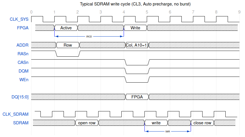
This is fairly similar to reads; the row is opened the same way, with an Active command (RASn goes low), then after tRCD has elapsed the FPGA drives the DQ bus with the data to be written, sets the DQMs and issues a Write command (CASn and WEn both go low). The SDRAM latches the data, writes it to the row, and then once tWR has elapsed it closes the row.
Interleaving multiple write commands is also pretty straightforward:
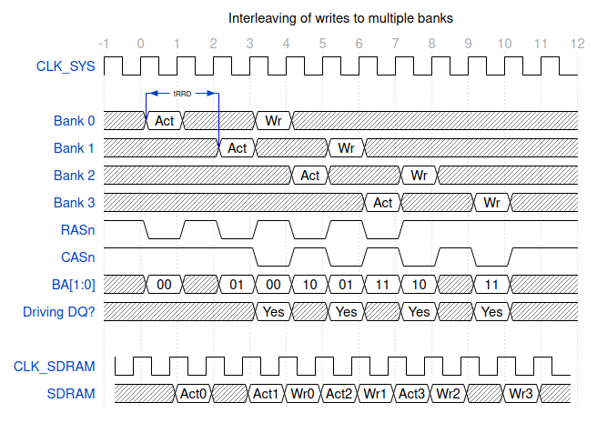
Once again we’re playing a Tetris-like game of “fill every idle slot”, and if we have a bunch of back-to-back writes to perform we do pretty well.
Where things get a bit messier is when we have to mix reads and writes. They have a different “shape”, so don’t interleave as neatly. It’s also very important that we don’t end up with both the FPGA and SDRAM chip driving the bus at the same time.
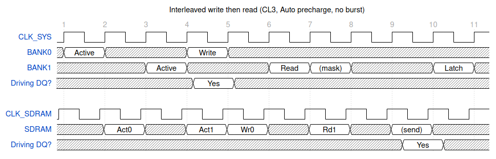
Write followed by read is no problem – it all fits, even though we end up with a few unused cycles:
Read followed by write is a bit trickier. If we follow the strategy of simply packing in the instructions as tightly as possible, we end up with this:
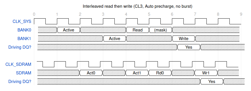
There are two problems here. The first is that, while this patterns works fine on a large number of SDRAMs, it doesn’t work in the Micron simulation model I’ve been using in development, and it also doesn’t work on the Winbond W9825G6KH chip on the Chameleon64V2 hardware.
The other problem is that because we have the FPGA and SDRAM driving the bus on adjacent cycles, we run the risk of bus contention.
Let’s take a closer look at how the SDRAM chip actually drives the bus.
When idle, both chips will have their output drivers disabled so the bus will be high-Z. When responding to a Read command, the SDRAM chip will place valid data on the line tAC after the clock edge, which is typically between 5.5 and 6ns. That does *not* mean that the bus remains high-impedance until that moment, however. The SDRAM’s output drivers are enabled almost immediately after the clock edge – tLZ is typically 1ns or less – and can be 0ns. While the data’s only guaranteed to remain valid for tOH after the clock edge, the bus remains driven until tHZ. So there’s a significant period either side of the valid data window where the SDRAM’s driving the bus.
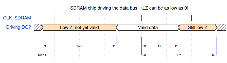
We should therefore be very careful about writing to the bus in adjacent cycles – if we do that, it should be timed very carefully (taking into account phase shifts between the clocks and any board delays) to avoid contention – and at higher speeds this may not be possible.
For this reason, the controller I describe in this series will sacrifice some potential throughput in the name of safety, and when a read is followed by a write, two potential slots will be left empty.
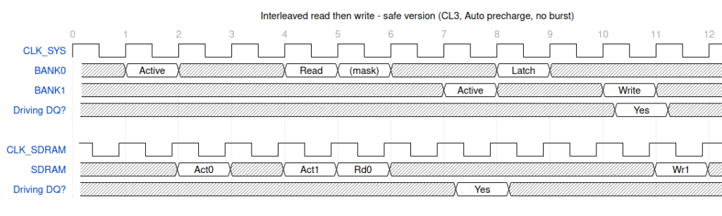
(Note that I’m actually delaying the write by one cycle more than is strictly necessary – the timing requirements of the core this controller’s supporting are extremely tight, and it helps to keep the controller operating on all even cycles, or all odd cycles.)
Next time I’ll look at port priority handling, request dispatching and ways we can meet the rather strict timing requirements of a 128MHz clock.