This is my first blog post in more than eighteen months, and while I’ve not been nearly as active tech-wise as previously, I am still porting cores to the Turbo Chameleon 64 (see https://www.patreon.com/coresforchameleon), and more recently I was kindly offered a prototype of the new SiDi128.
Normally I’d have declined, since most of the new FPGA platforms are far too complex for my tastes – but SiDi128 is oldskool. No Linux subsystem here – instead there’s an ARM microcontroller running a tight baremetal firmware which is an evolution of that used on the MiST, which itself can trace its origins back to the original Minimig. The FPGA is nice and big (nearly five times the size of the one on MiST) and the board has dual independent SDRAMs. In other words, a nice incremental improvement on the MiST without an explosion in complexity.
Slingshot on atari-forum, who is the primary core developer on MiST and SiDi128, had already ported the Minimig core to the new platform, and added support for the dual SDRAMs, placing Chip RAM, Kickstart, and slow RAM in one chip, and fast RAM in the other.
The expectation was that this would yield a nice performance boost – but it didn’t.
I changed things around so that Zorro II memory (used for RTG) was in the first RAM, then the whole of the second RAM would be the primary block of fast RAM – expecting RTG performance to improve significantly, since there would be less contention between the framebuffer and the software which was filling it.
Again, very little difference. What gives?
It occurred to me that if we were dealing with software rather than hardware then we would be looking to profile the program, to see where the hotspots were – perhaps I could do something similar in the FPGA?
So I wrote a module to count how many cycles elapsed between each “clkena” pulse, and build a histogram to show me how long various types of access were taking.
[As a brief aside, I should give a shout-out to the Altera/Intel SignalTap infrastructure and its Tcl scriptability. Tcl gets a lot of hate in the tech world, because of its quirky syntax – and I have to admit when I first encountered it I loathed it. But once I came to understand which type of bracket should be used where, and started to appreciate the elegant simplicity and minimalism behind its design, that loathing gave way first to a grudging respect, and eventually outright admiration. I especially appreciate that the Quartus Tcl scriping hosts (including quartus_stp) have a complete enough Tcl implementation that you can use Tk for basic graphical reporting.]
Since the CPU runs on the 113MHz clock but is kept in sync with the 28MHz clock, I was expecting to see cached accesses taking 4 cycles and other cycles that needed to access SDRAM taking 12 or 16 cycles, with occasional accesses taking longer.
That’s not what I saw. The vast majority of accesses were taking 4 or 8 cycles, which means RAM itself wasn’t being accessed very frequently at all. That was good news – it meant the cache was doing its job quite well.

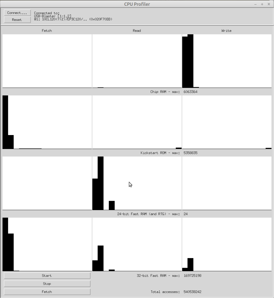
Here’s the profiler’s output window, showing the memory access statistics for DoomAttack. The histogram buckets are four cycles wide, since the CPU was kept in sync with the 28Mhz clock.
The first row shows chip RAM accesses, which are nearly all writes (as expected, since the game’s code and data is all in fast RAM.) Around half the writes are taking four cycles, and around half are taking eight cycles.
The second row shows ROM accesses, which is why they’re nearly all instruction fetches. The third row is largely irrelevant since it shows 24-bit RAM accesses, and there are very few of those happening during the course of the measurement.
The last row shows 32-bit fast RAM accesses, with the first histogram showing instruction fetch cycles, the second showing data fetch, and the third showing writes. A significant number of all types of access were taking eight cycles – so my goal was to try and reduce that.
This core has always been somewhat fragile timing-wise, and what I hadn’t realised was that in order to reduce timing pressures from block RAM to CPU, the cache is effectively two levels deep. There’s a respectable “level 2” cache of a two-way design – or rather two of them, one for instructions and one for data; but there’s also a very small “level 1” cache, just a single cacheline long, which is implemented as logic rather than block RAM. If a memory access hits the level 1 cache it can be served within four cycles. If it needs to fetch from level 2 then the access will take eight cycles.
Unfortunately, since there was only a single cacheline, it would have to be evicted and refilled any time the CPU swapped between instruction and data accesses. Fixing this was fairly straightforward, so we now have a separate level 1 cacheline for instructions and data.
I also tweaked the timing of write cycles so that more of them can be acknowledged within four cycles.
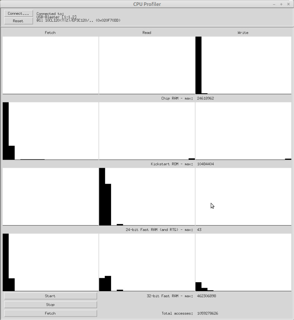
Those two changes made a significant difference to the framerate in DoomAttack, and the improvement is immediately visible in the profiler’s output:

Notice in particular that nearly all the chip RAM writes are now happening in four cycles.
The other improvement I wanted to make was to decouple the CPU from the 28MHz clock. From other projects I knew that when the CPU runs an internal (non-memory) cycle, it can be allowed to continue after three cycles rather than four, and when fetching from level 2 cache it should be able to continue after six cycles rather than eight. These changes also made a significant difference to overall performance.
Finally, to improve RTG performance, I changed the SDRAM controller to allow back-to-back bursts for the video system, nearly doubling the maximum theoretical bandwidth. This makes modes such as 1280×720 in 16 bit and 1440×900 in 8 bit much more usable.
As always, this has been quite the learning curve – and this time the main lesson learned is that there’s no substitute for measurement!
