
Things are getting interesting with the ZPU core, and it’s now pretty much where I want it for inclusion into other projects.
For use as a ROM loader in the PACE project I needed something that wouldn’t eat either too many logic elements or Block RAMs, and the ZPU looked to be the ideal candidate. It may also be possible to use it as an IDE-to-SD Card bridge for certain older projects that expect to run from Compact Flash card, but time will tell.
My first experiments with loading files from SD card worked out fairly well, but the code size was quite large – I was struggling to stay within 8KB (16 M4K blocks!), and had not a hope of squeezing it into 4KB. A big part of the problem was the emulation block at the beginning of the ROM. The first kilobyte or so in a ZPU program is devoted to software implementations of the optional instructions. Whether this code is ever used depends upon which variant of the CPU core is in use, and also which compiler flags are supplied when building the program, so my goal over the last few days has been to eliminate the need for emulated instructions in the Boot ROM without bloating the ZPU itself too much.
It’s possible to prevent the compiler emitting some of the optional instructions, by way of the -mno-??? switches. A complete list can be found by typing “zpu-elf-gcc –target-help”.
The first snag is that the pre-compiled toolchain has a bug which prevents the -mno-neg switch from working. I’ve submitted a patch, and the repo here contains the fix, but there’s no fixed binary as yet.
The -mno-*shift* flags also don’t work, and cause GCC to throw an internal error instead of emitting equivalent code. This means that in order to remove the emulation table I have no choice but to implement the shift instructions in HDL. This I have now done, along with a few other instructions. If I ask the compiler not to emit a select few instructions, like so:
-mno-poppcrel -mno-pushspadd -mno-callpcrel -mno-byteop -mno-shortop -mno-neg
Then I can get away with omitting the exception table, provided I don’t use division or modulo in the Boot ROM.
In combination with enabling “relaxation” while linking, by supplying the following argument to the linker:
-Wl,--relax
the Boot ROM is now under 4k.
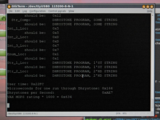
The Boot ROM currently loads a splash screen into SDRAM, then loads and runs dhry.bin, which does a Dhrystone benchmark and prints the result to the RS232 serial port.
The CPU itself now takes just under 965 logic elements, runs at 133Mhz and turns in a shade over 1.5 DMIPS when running from uncached SDRAM.
The entire SoC with CPU, SDRAM controller, VGA controller, SPI and UART takes 2001 logic elements.
For anyone interested in playing with this, source is on my GitHub page, and I’ve also made a binary snapshot for the DE1 board, based on this tag.
(Put dhry.bin and splash.raw on an SD card, and upload the .sof file to the DE1 board.)
Hmmm… with the ZPU being stack-based the data access patterns should be fairly simplistic. I wonder if a (very) small data cache, organized as “rotating barrel” (in lack of a better word) wouldn’t have a very nice hit rate. E.g., 256 32-bit entries, one 8-bit value denoting “bottom”, one 8-bit value denoting “top”. Push would store another entry in the cache and advance top, on wraparound bottom would be advanced etc.
Would obviously inflate the core 😉
Yes, I’m sure you’re right – and it’s certainly something to play with.
As it’s currently arranged, this version of the core has the stack in Block RAM, so the stack is already very fast, but it would be very interesting to look at making the stack automatically copy its contents to SDRAM on wraparound to make the stack effectively unlimited in size.
Ah, it appears I didn’t read deep enough to notice that the stack is not in SDRAM – I thought that every push/pop operation would go basically “unfiltered” to memory. 😉
1.6 DMIPS at 133 Mhz (is this FPGA clock or “effective” ZPU clock? I’m unexperienced in FPGA development, but I think I recall that, e.g., the TG68k core usually runs at a much lower effective clock than the FPGA and wonder if this is also the case for ZPU) sounds pretty anemic. Is this mostly bottlenecked on fetching instructions and operands?
That’s the thing with the ZPU – there are multiple implementations, so it’s hard to keep track of which variant does what! I haven’t helped by introducing yet another variant! The “full” version of the core *does* put the stack in external memory.
The traditional “small” version of the core has both stack and program in Block RAM, and can only access external addresses via load and store, for IO operations.
My variant of the small ZPU has (optionally) more instructions implemented in hardware, and can execute instructions either from Block RAM or external RAM.
The ZPU runs at the full sysclock speed (though I pulled that back to 125MHz for reliability.) And yes, 1.5 DMIPS is a bit weedy – that’s partly because I haven’t implemented loadb / loadh (The ZPU’s weakest operations are byte reads and writes, which dominate the Dhrystone test.), partly because instructions are being fetched from uncached SDRAM (the core can manage nearer 6 DMIPS running from Block RAM) and partly just the inefficiency of the stack-based architecture compared with a register-based CPU.
I suspect that with a 32-bit-based workload and a decent cache on the SDRAM, the ZPU would perform rather better.
Thanks a lot for elaborating, this is very interesting!