
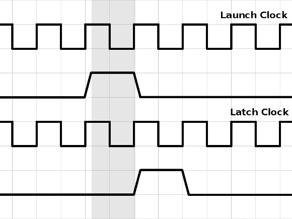
When designing a system with various virtual components all within an FPGA, transferring data from one module to another is fairly straightforward. Provided the two modules use the same clock, we simply send outgoing data on a rising clock edge, and sample it in the receiving module on the following rising clock edge. The new data has a complete clock cycle in which to propagate from the source to the destination.
Things become more complicated, however, when the modules aren’t in the same chip. A typical example is making an FPGA-based project communicate with SDRAM.
So why are things so much more difficult when one of the devices is external? In short, delays. Routing delays, delays due to capacitative loading, setup-and-hold delays, rise-and-fall delays. Each of these delays reduces the window of opportunity for sampling valid data, and the narrower that window becomes, the more carefully we have to control the timing of our FPGA project.
In the example depicted above, the shaded area represents the time window during which the destination could have sampled the high level of the source signal and received valid data. This window is very nearly a complete clock cycle in width, and in the example we’ve sampled it right at the end of the window. While it might look like this is too close for comfort, the slight delays as data travels from cell to cell in the FPGA effectively shift the data slightly in time, and the FPGA synthesis software automatically takes care of skewing clocks and inserting extra delays where needed to ensure the data is valid at the clock edge.
Now consider what happens when we send data to an external SDRAM. We must subtract the receiving device’s setup time and the receiving device’s hold time from this window. The valid data window is now much narrower, and our rising latch clock now falls outside that window, so we can’t rely on the sampled data being valid.
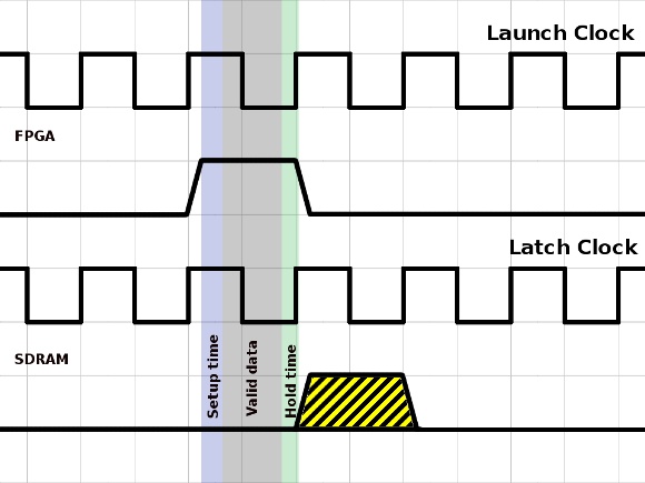
The solution to this problem is to phase-shift the SDRAM’s clock, so that the rising edge falls within the valid data window. On most FPGAs this is really easy – instead of running the design and the external device from the same clock, we can use a PLL to create two versions of the clock, one phase-shifted slightly.
Problem solved?
Well… no!
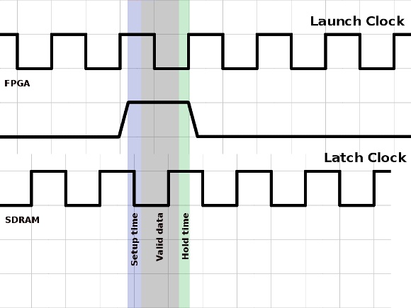
We’ve taken care of sending data to the external device, but what about receiving data? When sending data in the opposite direction the SDRAM’s clock becomes the launch clock, and the FPGA’s clock becomes the latch clock, which means that the phase shift now delays rather than advances the latch clock. There’s no way data launched at the SDRAM’s clock will be ready for the next rising edge of the FPGA’s clock, since they’re very close together – so we must shoot for the clock edge after that. But that’s more than one complete clock cycle away. Is it possible to meet that target?
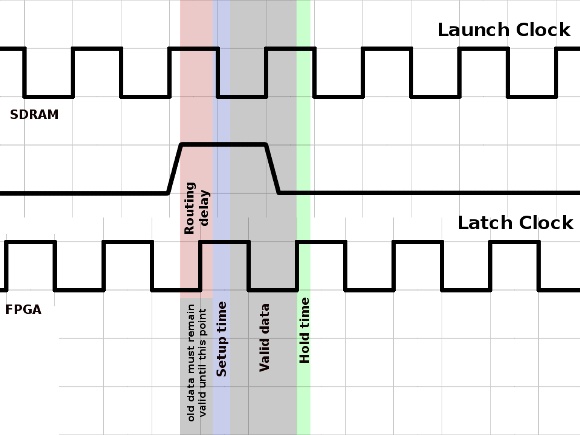
In the case of writing to the SDRAM, we didn’t have to worry about routing delays, because the delays on the signals and the delay on the clock should be roughly equal, and should thus largely cancel each other out. However, when transferring from SDRAM to the FPGA they no longer cancel out, they combine. This delay actually helps us out, by shifting the valid data towards the clock edge we’re aiming for. There are also input delays at the FPGA, and as long as the synthesis software is given enough information about timing requirements, it will insert extra delays to help align the latch clock with valid data.
Specifying timing constraints in Quartus is a bit of a black art and finding information on the subject is not easy. The following is my own understanding on how to specify timing constraints from within Quartus – I may have misunderstood some of it, so don’t take this as Gospel, but it seems to work in my own projects.
To begin with create a new Synopsis Design Constraints file, and save it, add it to the project, and on the Assignments -> Settings dialog, go to the TimeQuest Timing Analyzer page, and add the newly created file to the list of SDC files for the project.
So let’s go through a typical .sdc file line-by-line:
#**************************************************************
# Time Information
#**************************************************************

set_time_format -unit ns -decimal_places 3

#**************************************************************
# Create Clock
#**************************************************************

create_clock -name {clk_50} -period 20.000 -waveform { 0.000 0.500 } [get_ports {iSYS_CLK}]
This defines a master clock of 50 MHz (period 20ns), coming into the project on the toplevel pin called iSYS_CLK. In most of my projects this clock isn’t used for anything directly – it’s fed into a PLL which generates the real clocks.
#**************************************************************
# Create Generated Clock
#**************************************************************

derive_pll_clocks
Rather than specify the PLL clocks individually, we can have them automatically analyzed and generated.
However, it’d be useful to refer to the SDRAM clock by name, so next we’ll create that one explicitly.
The path of the PLL counter will depend on the name you’ve given the PLL, and also the device you’re using: This example comes from a project which targets a Cyclone II – the path will need adjusting for other devices:
create_generated_clock -name sd1clk_pin -source [get_pins {mySysClock|altpll_component|pll|clk[1]}] [get_ports {sdr_clk}]
(If you right-click within the Quartus text editor while editing an SDC file, as long as TimeQuest is currently open, you can use the Insert -> Generated Clock menu item to help you find the correct path.)
#**************************************************************
# Set Clock Uncertainty
#**************************************************************

derive_clock_uncertainty;
Adds some margin-of-error to the clocks defined thus far.
Now we come to the trickier stuff. Here we need to refer to the datasheet of our SDRAM. We also need to make a rough estimate of our PCB routing delays. Assuming the SDRAM and FPGA are right next to each other and have only short traces between them, 1 ns wouldn’t be an unreasonable estimate.
I’ll take the following parameters for an IS42S86400B.
The parameters we need to know are:
- Min Output Time (Low impedance or output) – 0ns
- Max Output Time (High impedance or input – i.e. bus turnaround time) – 5.4ns
- Input Setup Time (often specified separately for address, data, etc. Take the largest.) – 1.5ns
- Input Hold Time (again, take the largest.) – 0.8ns
#**************************************************************
# Set Input Delay
#**************************************************************

set_input_delay -clock sd1clk_pin -max 6.4 [get_ports sdr_data*]
set_input_delay -clock sd1clk_pin -min 1.0 [get_ports sdr_data*]
Here we’re telling Quartus how long after the SDRAM’s clock edge we can expect to wait before valid data arrives at the FPGA. The only pins on the SDRAM that send data back to the FPGA are the Data pins, so the wildcards in the get_ports section reflect this.
For the maximum input delay we take the largest output time and add the estimated routing delay.
For the minimum delay we take the smallest output time and, again, add the routing delay.
#**************************************************************
# Set Output Delay
#**************************************************************

set_output_delay -clock sd1clk_pin -max 1.5 [get_ports sdr_*]
set_output_delay -clock sd1clk_pin -min -0.8 [get_ports sdr_*]
Here we’re saying that we have to have valid data on the lines 1.5ns before the SDRAM’s clock edge, and it must remain valid until 0.8ns *after* the clock edge, hence the 0.8 being negative. This applies to all SDRAM-related signals with the exception of the clock, so it’s a good idea to name the clock pin something that won’t be caught by the wildcard. Alternatively, you could specify these lines for each group of signals individually, instead of using such a wide wildcard.
Last but not least, we need to set a “multicycle path” to deal with the fact that we’re skipping a clock edge when reading data back from the SDRAM.
#**************************************************************
# Set Multicycle Path
#**************************************************************

set_multicycle_path -from [get_clocks {sd1clk_pin}] -to [get_clocks {mySysClock|altpll_component|pll|clk[0]}] -setup -end 2
And that’s basically it. Having specified this file, rebuild the project, then run TimeQuest.
From within TimeQuest, run the “Report all IO timings” report, and see if any of them are failing. If they are, adjust the phase shift on the SDRAM clock, which will probably end up being somewhere between about -0.5ns and -2.5ns.
Great paper on time constraints! I’ve never quite got the topic, now there is some hope.
Glad you found it helpful. I’m still hazy on the finer points myself – but I find there’s no better way to crystallize your understanding of something than to try and explain it to someone else! 🙂
Hey,
Great job I found this helpful! I”m actually trying to figure out TimeQuest now. Do you know what you do if you use something like parallel flash and don’t have a clock going to the external memory device? For example, my flash part only needs address, data and control lines, but no clock. I can’t find much direction as to how you constrain something like this.
Hi,
Great job! I found this helpful as well 🙂 but still has some doubts regarding the set output delay for source asynchronous devices! For example, if my data lanes are delayed in relationship with the clock from the source async device perspective, and at the some time got a time violation. could I use this as an input to the tool ?
set_output_delay -clock sd1clk_pin -min -1.5 [get_ports sdr_*]
set_output_delay -clock sd1clk_pin -max -1.0 [get_ports sdr_*]
From your perspective, What does this mean ? can you explain it as a pratical case of use ?
I haven’t actually worked with asynchronous devices, so I’m probably the wrong person to answer this. Having said that, the two commands you’ve listed there specify that the data must be valid for at least 1.5ns after the clock edge – but if the device is asynchronous what are you using as a clock? If you have some kind of strobe signal then you can probably use different output delays on the strobe vs. data lanes to ensure the relative timings between the two are maintained – but it’s not something I’ve explored.
Hi, Nice description on the topic. This was very helpful.
Thanks for clearing my concepts.
set up and hold times in your picture are with respect to which clock edge? it looks like they are with respect to negative edge of latching clock. is that right?
Apologies for not responding sooner. All times are with respect to the rising edge of the appropriate clock. In the last diagram, the fact that the rising edge only just falls within the valid data illustrates why as the clock speed goes up getting the timing constraints right is so critical.
Hello AMR
Did you apply multicycle constraint after running TimeQuest at least one time and seeing that there are violations … or it was clear at once that multicycle is necessary ?
Thanks
A bit of both – I had violations in the TimeQuest report but when I investigated it was clear that the SDRAM controller was waiting one extra clock before latching the data compared with what you’d expect from the SDRAM’s datasheet.
Amazing!
I was looking for that explanation for a while!
Excellent work!
Thank you very much!
Excellent work here !
Can you confirm that set_input_delay -max or -min and set_output_delay -max or -min provide only information to timing analysis, and do not create any delay ?
But I think it’s also possible to phase shift the CLK without PLL with set_output_delay (…) -add_delay 1.000 (…), for 1ns delay, you can confirm that too ? I imagine it’s less precise than PLL phase shift. It’s working in my case @125MHz, but with no timing analysis, so I’m not 100% confident…
I think the truth’s more complicated than a simple yes/no. The timing constraints don’t instruct the tools to add any specific delay (they simply inform the tools of delays which exist, but which the tools wouldn’t otherwise know about) – but if timing is failing, I believe the tool might add some routing delay in an attempt to make timing succeed.
Likewise, adding delay to the clock signal with set_output_delay shouldn’t phase-shift it, but perhaps it might prompt the tools to add some routing delays to other signals related to that clock. It’s likely to be unpredictable, though.
Thanks a lot for answering, and thanks again for your demystifying job, most of the time just length of Data and Address are considered : as you, I can see that with 6ps/mm it’s not usefull at 100MHz, but the CLK shift is essential, but I didn’t well finish the job as you’ve done here !.
After lots of experiments (with scope), I’m now sure that “-add_delay” really add delay, but all others don’t seem to add delay, but “the tool is routing delay in an attempt to make timing succeed” can be true too, I don’t test yet these cases.
At the end, my decision is now not to use the timing analysis, but adopt a practical method : I use a PLL_OUT as SDRAM clk, I will try to find the phase shift limit between SDRAM don’t work perfectly and SDRAM work perfectly (with a special test with thousands of Read/Write), and after find the phase shift limit between SDRAM work perfectly and SDRAM don’t work perfectly. And then I choose the pahse shift value between these 2 limits 🙂