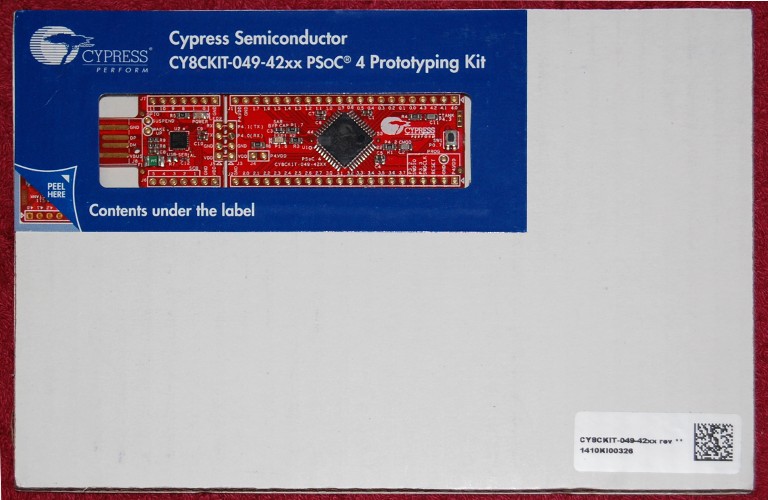
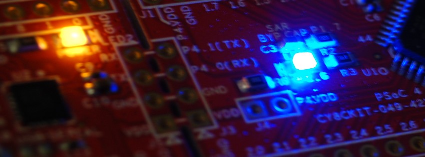
I have a new toy to distract me from my existing projects!
I recently came across this neat little prototyping kit from Cypress Semiconductor, and several aspects of the device piqued my interest:
- The cost is low enough that you don’t have to think twice about using one in a project
- The chip has an ARM Cortex M0 CPU core
- The 42xx version (as opposed to the 41xx version) has a small amount of FPGA-like programmable logic built in
- The device is programmed via an onboard USB/TTL converter, which in a piece of superbly elegant design can be “snapped off” the board once programming is complete.
- The device is capable of running from 5v, and handling 5v signals.

I just had to get hold of a few of these, so after a brief search for somewhere that sells them individually and doesn’t want a fortune for postage, I bought a few of them from DigiKey. I already have a project or two in mind for them, and will write about them here as work progresses.
The device comes packaged in a cardboard slab with a hole cut out for the circuit board – simple but effective. There’s no CD, so you have to download the software on-line. The software is free and seems to be powerful and flexible without having too horrible a learning curve. Unfortunately there is no support for Linux, so I had to press my rather creaky old WIndows XP partition into service.
One hurdle that took some figuring out: the “Bootloader Host” part of the software, which is required in order to upload a design into the chip, doesn’t work on com ports numbered 10 or above, so it may be necessary (and was on my machine) to force the virtual serial port this device provides to be a low-numbered COM port. (On my machine the only available port below 10 was COM2, so I used that.)


An interesting little platform, which seems to be quite powerful (48 MHz CPU, up to 4 KBytes of SRAM, up to 32 KBytes of Flash – and the reconfigurable blocks I have no actual feeling how powerful they are). Being able to work with 5 Volts is also nice.
Do you think that this platform could be used to develop replacements for some aging chips such as the MOS 6526 (the C64’s CIA, which is susceptible to ESD damage) which are increasingly hard to find?
Actually, the 6526 may need 38 GPIOs, this platform has only up to 36 GPIOs, so this may not actually work out in this case.
That’s an interesting idea, and may well be possible. I think the logic would be a tight fit, but I think it would fit.
Regarding GPIOs, I would think TOD could be derived from the ø2 clock, saving one pin. One of the CIAs doesn’t need /PC either, but I’m not sure what could be saved from the other one. I suppose the other option might be to run the chip entirely from its built-in clock, and ignore ø2 as well, just synchronising the chip using /CS?
Yeah, TOD looks easily derivable from phi2, but ignoring phi2 sounds very tricky 😉
What a pity, one pin missing…
I’m not sure it’d be that tricky – looking at the datasheets and schematics, I think it’d be possible to generate a clock of 8Mhz or so, sample /CS from that clock domain and use it to time the read and write cycles. Could certainly be an interesting project!
Hmm… according to http://www.c64-wiki.de/images/2/21/Schaltplan_C64_original.pdf (and provided I read things correctly) there may be some pin-savings for the serial bus: DATA and DATA OUT end up leading to the same line on the bus, as do CLK and CLK OUT. Provided their usage is mutually exclusive, perhaps one can get away with one pin each by switching in- and output appropriately?
Interesting! Sadly, U8 is an inverting buffer, which makes it impossible to share the input and output functions in this way. The data and clock inputs on the chip are open collector with pullups on the motherboard, so devices on the serial bus drive them low but don’t actively drive them high. A PSOC-based replacement chip would have to drive the pins in “open-collector, driving low” mode, and the line’s status would only be readable while the pin’s set to logic high. Unfortunately U8 would invert that logic high state and drive the line low! If U8 weren’t inverting, then those pins could indeed be shared.
Ah, what a pity. I noticed the inverters and just though “well, then let’s just output a 0 if we really want a 1” – but that’s obviously not how things work in that area 😉
Thanks for elaborating!