
2021-06-23
To recap, I had chosen the MiST Megadrive/Genesis core as my next project in porting to Turbo Chameleon 64 – in theory a simple task since the core leaves enough logic and block RAM free to simply bolt on the DeMiSTify component and go.
Except…
Well, nothing’s ever simple, is it? The port worked fine on the Turbo Chameleon 64 V1, worked fine on DE10-lite, and failed on Chameleon 64 V2.
The problem was stubbornly resistant to the adjustment of phase shifts, and even reducing the entire project’s clock speed – so I was going to need to rig up a testbench – one that could run both in simulation and on real hardware – in order to track this down.
The SDRAM controller in the Megadrive core has multiple access ports, and I already knew from having written a simple Megadrive ROM for testing that the problem wouldn’t show unless memory was being exercised fairly hard. Therefore I needed to create a complex write/read pattern for many ports simultaneously.
In the past when testing SDRAM I’ve made use of Linear Feedback Shift Registers, since they generate a stream of values which look pretty random, but which are entirely predictable and repeatable, and best of all, only emit each value once during the length of their cycle. That means I can write to RAM using a sequence of LFSR-generated addresses, then verify the written data by repeating the sequence and reading from RAM.
The ports on the controller vary in both address and data width, however, which means I need to use LFSRs with differing parameters. In the past I’ve always rigged up the LFSR on an ad-hoc basis, using an old Xilinx application note for reference, but this time I wrote a more generic LFSR module to be incorporated into this and future projects; I must admit I went down a bit of a rabbit-hole here, and ended up with a parameterised module which supports LFSRs with a width of up 128 bits. It also supports saving the register’s current state and recalling it – so that a sequence can be replayed from any point, not just from the initial seed value. So (any typos in the tap lists notwithstanding) LFSRs are probably not something I will have to think about again
I set up a porttest module which uses a state machine to write a sequence of “random” length, with “random” values to “random” addresses, then reads the same sequence back from RAM to verify it. Again, this is parameterised so it can be made to fit the various ports in the SDRAM controller. The idea is to make sure the controller is exercised with a good mix of simultaneous reads and writes, to test every combination of command sequencing.
In order to get a clear idea of what’s going on it’s helpful to be able to simulate the testbench, and to do that a model of the SDRAM is required. Micron supply a nice verilog model of their SDRAM chips here – but as written it’s not compatible with Verilator. Luckily György Szombathelyi (who’s done a huge amount of work on MiST cores in recent years) tweaked the model for Verilator-compatibility when working on the Minimig SDRAM / Cache implementation, so with those modifications included, and with a few more minor tweaks to how it handles tri-stating, I can run my testbench in simulation.
And I see read errors.
Here’s a trace of the first error being detected:
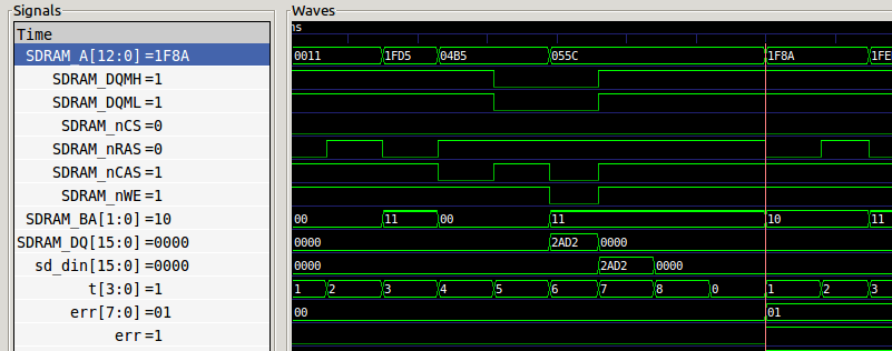
The SDRAM chips used on the platforms of interest contain four banks, which act almost like four independent chips sharing a single bus. Even though it takes several cycles to open a row, issue a read command to a particular column and to receive the data, with careful scheduling of commands much of the overhead can overlap, making it possible to transfer data extremely efficiently. In the best case, data can be transferred every cycle.
The SDRAM controller used in this core makes extensive use of bank interleaving – which is just as well because there are eight different subsystems making simultaneous demands of the SDRAM!
The sequence in the trace above shows a row being opened for access, first on bank 0 then on bank 3. This is followed by a Read command on bank 0 (the first time CAS goes low), then a write command on bank 3 – however the read command is failing in simulation. The reason for this is that the model doesn’t support the write command being issued in between the read command being received and its data being sent – the write command appears to be preventing the read from writing to the bus.
The testbench fails at exactly the same point on real hardware – but not *all* real hardware. Specifically, it works fine on every board I’ve tested so far (MiST, Turbo Chameleon 64 V1, DE10-lite and a cheap Cyclone IV board bought from EBay some years ago), and fails on Turbo Chameleon64 V2 and QMTech’s newest Cyclone IV board. What these latter two devices have in common is the SDRAM chip – they both have a Winbond W98G256KH-6. (The V1 Chameleon also has a Winbond chip, but it’s an earlier and faster version.)
So while I don’t have actual proof, at this point I believe that, like the verilog model, the newer Winbond chip simply doesn’t support that particular access pattern, and re-writing the controller to avoid it fixes the problem, both in simulation and on real hardware. I suspect – though again I have no proof – that this access pattern isn’t actually valid at all, and just happens to work on most chips as an implementation quirk. None of the datasheets I’ve read so far make any mention of this pattern – though admittedly they don’t forbid it either – however the fact that the DQMs on the write command also affect the second word of the read gives a hint that it might be troublesome.
The upshot of all this is, however, that for some projects I will need to have different versions of the SDRAM controller for different boards, which is a something I’d hoped to avoid.
Next time I’ll talk about adjusting and re-writing the controller to avoid this pitfall.