
Part 1 – 2021-07-04
In my last post I talked about the need to adjust the SDRAM controller used by the Megadrive core to make it work on the TC64V2, and having released that port it was time to turn my attention to the PC Engine core.
This one has actually been on the back burner for months. I started to port it at the beginning of the year, found that it didn’t work on TC64V2 and didn’t yet understand why not. With plenty of other projects to keep me busy I neglected this one for a while, but revisited it recently, armed with fresh knowledge about why it wasn’t working.
Adjusting the SDRAM controller on the Megadrive core wasn’t too difficult – I had to a sacrifice a bit of potential throughput in order to avoid the Read/Write/Data access pattern which wasn’t working on the newer Winbond chip – but the PCEngine core’s SDRAM controller has even more stringent timing requirements and a state machine which takes multiple paths in order to keep the response time as low as possible. Adapting this one would be much harder.
Instead I re-wrote it largely from scratch, since I wanted to take a different approach.
An SDRAM controller, broadly, has to perform three tasks. It has to initialise the chip, it has to arbitrate between the various subsystems which want to use the RAM, and it has to perform the actual data transfer to and from the chip.
For the PC Engine core it needs to do this at 128MHz, it can’t keep the VRAM ports waiting or there’ll be graphical glitches – oh, and it has to squeeze in some refresh cycles, too, otherwise the RAM contents will be prone to corruption.
Good thing I like a challenge, isn’t it?
So let’s take a look at a typical SDRAM read transaction.
SDRAM chips can transfer data in bursts of 1, 2, 4 or 8 words, or they can transfer an entire page at a time. It’s possible to use single words for writes while using bursts for reads, and it’s possible to terminate a read or write burst in progress if you only want part of it. We can also choose whether data arrives 2 clocks after a Read command is registered by the RAM, or 3 clocks. CAS Latency 2 (CL2) mode is typically only available at speeds up to about 100MHz, but some chips (including the Winbond device in the TC64) can do CL2 up to 133MHz.
The PC Engine core doesn’t make use of bursts, we’re only transferring a single word at a time which will make this analysis simpler. (The Megadrive core uses 2-word read bursts, which is also fairly simple to deal with.)
So here’s what a single read transaction looks like from the point of view of the FPGA, and from the point of view of the SDRAM chip, and also of the data bus. Note that the SDRAM’s clock is slightly ahead of the FPGA’s system clock – this phase shift is important.
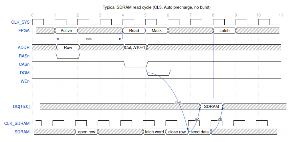
So what’s happening here is that the FPGA’s launching a “Bank Active” command (RASn goes low) to open a particular row of data. The 32 meg SDRAMs on the target boards have 13 address pins, allowing 8192 rows per bank, so we use the full address bus to select a row.
After tRCD has elapsed we can issue a command to the newly-opened row, so we drop CASn and set the address bits appropriately. The chips use address bits 8:0 for the column address (64 meg chips would use A9 as well), while bit 10 has a special meaning: auto-precharge. Precharging is the act of readying the bank for opening a new row. If bit A10 is set when we issue a read or write command, the chip will automatically close the row at the earliest opportunity. If A10 is clear then the row remains open, and we’re free to issue another read or write command to the same row, and we can issue a Precharge command if we want to close the row manually. In this case we’re making use of autoprecharge, so the row is closed immediately after the read has been performed.
The DQM signals are of particular note. Firstly, there are two of them – one for each byte within a word, and they can be used to mask data, both while reading and writing. This makes it possible to write to just half of a word without corrupting the other half. There are two complications: firstly, the mask takes effect immediately on writes, but on reads it takes effect two cycles later. This means it’s necessary to take particular care when mixing read and write instructions. The other complication is that for reads, the latency of the DQMs is always 2 clocks, even though the data itself can have a latency of 2 or 3 cycles. Looking at the diagram, if DQM didn’t go low at clock 5, then the value being read wouldn’t be launched at clock 7, and wouldn’t arrive at clock 8.
Note also that there is a delay before the data is present on DQ bus. The data becomes valid at tAC (typically about 5.5ns) after the first clock edge, and remains valid until tOH (typically around 3ns) after the second clock edge. It’s important that we latch the data somewhere during this window of valid data, and fine tuning the timing to arrange this is the reason for phase-shifting the SDRAM’s clock with respect to the system clock.
Another thing to note is that just because the data isn’t valid until tAC after the clock edge, doesn’t mean the data bus remains high-Z until then. In fact the chip is already driving the bus (albeit with data that’s not yet valid) a mere tLZ (typically between 0 and 1ns) after the clock edge.
In the diagram above it took us nine cycles to read a word – that’s not exactly impressive performance. Luckily, there are tricks we can use to improve throughput. I mentioned in a previous post that SDRAM chips contain four banks, which behave pretty much like four independent chips sharing an interface. It’s clear that in the diagram above there are a number of idle cycles, and we can use those to issue commands to other banks.
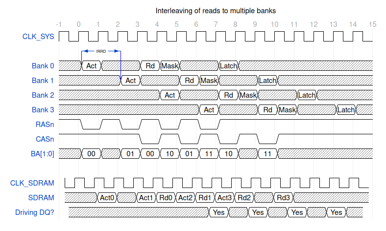
Here we issue a command to each bank in turn. I haven’t shown all the control signals here, but notice how RASn and CASn are alternating quite neatly. Since the Active command (RAS) doesn’t care about the state of the DQMs, it’s fine to be masking another bank’s transaction while issuing an Active command (unless you’re using a MiSTer memory module – that’s a story for another time!).
At clock 10 we could issue a new Act command to bank 0 and repeat the cycle, so we could consistently transfer four words every 10 cycles. That’s a significant improvement. If we were using 2-word bursts, we’d be transferring data on 8 out of 10 cycles.
Next time I’ll look at write cycles, and the care required when mixing reads and writes – and maybe talk about the controller itself.