When designing a system with various virtual components all within an FPGA, transferring data from one module to another is fairly straightforward. Provided the two modules use the same clock, we simply send outgoing data on a rising clock edge, and sample it in the receiving module on the following rising clock edge. The new data has a complete clock cycle in which to propagate from the source to the destination.
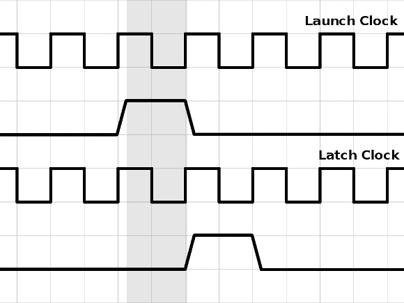
Things become more complicated, however, when the modules aren’t in the same chip. A typical example is making an FPGA-based project communicate with SDRAM.
Continue reading