Demystifying Timing Constraints

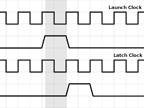
When designing a system with various virtual components all within an FPGA, transferring data from one module to another is fairly straightforward. Provided the two modules use the same clock, we simply send outgoing data on a rising clock edge, and sample it in the receiving module on the following rising clock edge. The new data has a complete clock cycle in which to propagate from the source to the destination.
Internal

Things become more complicated, however, when the modules aren’t in the same chip. A typical example is making an FPGA-based project communicate with SDRAM.
Continue reading

Obscure obsolete media du jour

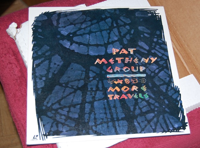
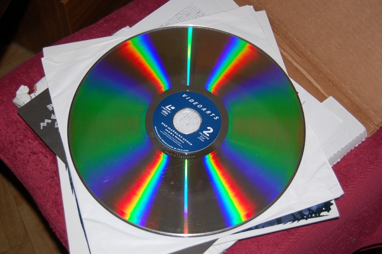
Having found that clip of the Pat Metheny Group on YouTube a couple of weeks ago, I wanted to get hold of the DVD from which it was ripped. Unfortunately it seems to be really hard to track down – I can find it easily enough on VHS, and also on Laserdisc, but not on DVD. So I acquired it by… ahem… “other means”. Since I’ve never actually handled a Laserdisc, though, I couldn’t resist the urge to buy a copy from a Stateside seller on EBay.

It arrived yesterday.

sleeve
Disc

It was wrapped in newspaper, and I can honestly say this is a headline I never thought I’d see:

Nuns

Some linker-script magic

In my last post I mentioned that I had to employ some ugly hacks in the boot firmware for my ZPU project, to make sure certain structures ended up in SDRAM rather than the initial Boot ROM.

To illustrate the problem let’s look at a minimal test program:

short inconvenience;

int main(int argc,char **argv)
{
    inconvenience=0x0123;
    return(0);
}

This little program declares a 16-bit word global variable, and then writes to it.  The assembly output produced by

zpu-elf-gcc -Os -S bsstest.c

is as follows:

    .file    "bsstest.c"
.text
    .globl    main
    .type    main, @function
main:
    im 291
    nop
    im inconvenience
    storeh
    im 0
    nop
    im _memreg+0
    store
    poppc
    .size    main, .-main
    .comm    inconvenience,2,4
    .ident    "GCC: (GNU) 3.4.2"

Note the storeh instruction half way down.  That’s the source of my problem.  I’ve implemented storeh in hardware for SDRAM, but not for the BlockRAM-based Boot code, and I’d really like to avoid doing the latter if possible, because doing a 16-bit write to a 32-bit wide RAM is going to be messy and eat up logic elements.  The boot code is also rather on the large side, so it would be nice to avoid storing unitialised data in there at all if possible.
Continue reading

A System-on-Chip in 2300 logic elements!

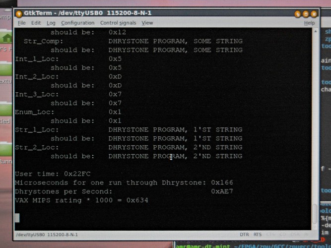
My experiments with the “small” variant of the ZPU processor have resulted so far in a reasonably functional and tiny System-on-Chip. Supported so far are:

  • ZPU processor with GCC toolchain support
  • SDRAM controller with cache
  • VGA video output, 640x480x16-bit (Dithered on DE1 board)
  • Millsecond counter
  • SD card access
  • UART
  • HEX display (DE1 only)

All within a mere 2300 logic elements.
Continue reading

More Follin Fandom

It doesn’t seem to matter which platform’s sound chip Tim Follin composed for, he always seemed to find some way of squeezing more out of it than anyone previously thought possible. Here are just a few examples, found on YouTube…
Continue reading