It’s Aliiiiive!

After spending a satisfying few hours tracking down a stubborn bug which turned out to be a mere bad solder joint, my old A500 motherboard is now able to boot using the Vampire500 board in place of the CPU!

FirstBoot

Unfortunately, since that means I can now play some old favourites on the board (in the name of testing, of course!) there probably won’t be much more progress today!

Pang

From the “What, are you nuts?” department!

I have an Amiga with a ZPU processor!

So what possessed me to create such a perverse combination? Quite simply that it synthesizes in about a third of the time that a TG68-based equivalent would, which speeds up the development cycle significantly while I’m bug hunting.

(I will admit there’s an element of “because I can” there, too!)

ZPUChipRAMTest

This not-very-exciting screenshot shows a simple program running on the ZPU, and testing the reliability of reads and writes to Chip RAM through the Vampire500.  The program simply sets up a 2-colour high-res screen, clears the framebuffer, and then repeatedly adds 1 to each longword within the framebuffer.  Any glitches in either reading or writing would thus be cumulative, so if I can leave the program running for a while and if the pattern on screen remains in nice neat columns (which it does), I can be sure that no glitches have occurred. (Or that any errors are perfectly consistent!)

Of course, a ZPU-based Amiga is of no practical use whatsoever, besides assisting in debugging the Vampire500 – but I find myself idly wondering how practical it would be to use a more modern CPU – such as, perhaps, the OR1200 – and then emulate the 68000 in firmware?

Anyhow, pipe-dreams aside, the next task will be to take a checksum of the Kickstart ROM, since ROM reads are the only kind I haven’t yet tested.

A New Distraction!

I have another new toy to distract me from all the things I should be doing!

Vampire500_InSitu

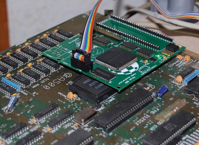
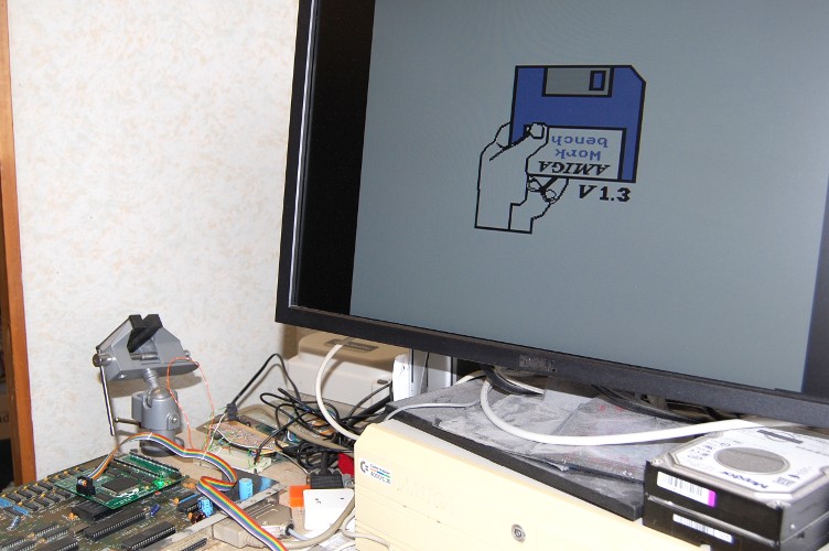
This is one of Majsta’s hand-assembled prototypes of his FPGA accelerator, connected to a spare A500 motherboard that I just happened to have lying around.  (I don’t currently have an A600 to play with, which is why Majsta sent me the less-mature A500 variant of the project).  While I’ve been trying to help with the SDRAM problems his project’s run into, there’s only so much I can do without access to the hardware.  Well, now I have that access!

The A500 variant of the project’s not yet as complete as the A600 version, and can’t yet boot from the TG68 processor, so now begins the fun of testing the various kinds of accesses to the A500 motherboard, and ironing out the glitches.

Because the whole project takes some time to build, while I’m testing and diagnosing I’m using a simple state machine to simulate the CPU, which looks like this:

library ieee;
use ieee.std_logic_1164.all;
use ieee.std_logic_unsigned.all;
use ieee.numeric_std.all;

entity DummyCPU is
    generic(
        SR_Read : integer:= 0;         --0=>user,   1=>privileged,      2=>switchable with CPU(0)
        VBR_Stackframe : integer:= 0;  --0=>no,     1=>yes/extended,    2=>switchable with CPU(0)
        extAddr_Mode : integer:= 0;    --0=>no,     1=>yes,    2=>switchable with CPU(1)
        MUL_Mode : integer := 0;       --0=>16Bit,  1=>32Bit,  2=>switchable with CPU(1),  3=>no MUL,  
        DIV_Mode : integer := 0;       --0=>16Bit,  1=>32Bit,  2=>switchable with CPU(1),  3=>no DIV,  
        BitField : integer := 0           --0=>no,     1=>yes,    2=>switchable with CPU(1)  
        );
   port(clk                   : in std_logic;
        nReset                 : in std_logic;            --low active
        clkena_in             : in std_logic:='1';
        data_in              : in std_logic_vector(15 downto 0);
        IPL                      : in std_logic_vector(2 downto 0):="111";
        IPL_autovector       : in std_logic:='0';
        CPU                 : in std_logic_vector(1 downto 0):="00";  -- 00->68000  01->68010  11->68020(only some parts - yet)
        addr                   : buffer std_logic_vector(31 downto 0);
        data_write            : out std_logic_vector(15 downto 0);
        nWr                      : out std_logic;
        nUDS, nLDS              : out std_logic;
        busstate                : out std_logic_vector(1 downto 0);    -- 00-> fetch code 10->read data 11->write data 01->no memaccess
        nResetOut              : out std_logic;
        FC                  : out std_logic_vector(2 downto 0);
-- for debug        
        skipFetch              : out std_logic;
        regin                  : buffer std_logic_vector(31 downto 0)
        );
end DummyCPU;

architecture rtl of DummyCPU is

type states is (write1,write2,write3,write4,write5,write6,read1,read2);
signal state : states := read1;
signal counter : unsigned(15 downto 0);
signal temp : std_logic_vector(15 downto 0);

begin

process(clk)
begin
    nResetOut<=nReset;
    if nReset='0' then
        state<=read1;
    elsif rising_edge(clk) then

        case state is

            when write1 =>
                data_write<=temp; -- std_logic_vector(counter);
                addr<=X"00DFF180";
                busstate<="11";    -- Write data
                state<=write2;
                nWR<='0';
                nUDS<='0';
                nLDS<='0';

            when write2 =>
                if clkena_in='1' then
                    state<=write3;
                end if;

            when write3 =>
                addr<=X"00BFE201";
                data_write<=X"0003"; -- Set OVL and LED as output
                nWR<='0';
                nUDS<='1';
                nLDS<='0';    -- Byte write to odd address.
                state<=write4;

            when write4 =>
                if clkena_in='1' then
                    state<=write5;
                end if;

            when write5 =>
                addr<=X"00BFE001";
                data_write<=X"FFFF";
                data_write(1)<=temp(6);    -- Echo mouse button status to keyboard LED.
                nWR<='0';
                nUDS<='1';
                nLDS<='0';    -- Byte write to odd address.
                state<=write6;

            when write6 =>
                if clkena_in='1' then
                    state<=read1;
                end if;

                when read1 =>
                addr<=X"00BFE001";
                busstate<="10";    -- Read data
                state<=read2;
                nWR<='1';
                nUDS<='1';    -- Byte read from odd address.
                nLDS<='0';

            when read2 =>
                temp<=data_in;
                if clkena_in='1' then
                    state<=write1;
                end if;

        end case;
    end if;
end process;

end architecture;

This state machine reads the value of CIA-A PRA and writes the value read to the COLOR0 register, so the colour of the screen changes in response to the mouse or joystick buttons. It also writes the status of the left mouse button to the LED bit, so the keyboard LED lights in response to the mouse button.

Next I shall test reads and writes to Chip RAM and reads from the Kickstart ROM for reliability.

Loading a JPEG with the ZPU

I’ve been playing around with the ZPU again, and exploring what’s needed to get such things as malloc() and rudimentary filesystem support working. By re-using the FAT filesystem code from the Minimig project’s firmware and creating a simple wrapper, I now have a complete enough system that I can load and display a JPEG file from SD card.

DSC_7288
An image in the process of being loaded

A 640×480 JPEG currently takes approximately 39 seconds to load and display – my next project will be to explore hardware acceleration of the DCT and see how much faster this can be made.

A binary snapshot with DE1 and DE2 bitstreams, and files to go on the SD card can be found here
The source repo is tagged to match this snapshot.

Generalizing the Boot ROM

With its tiny size the ZPU would seem an ideal candidate for a multi-core design.  Unfortunately, instantiating more than one of the traditional zpu_small cores in a single project is complicated by the ROM / Stack RAM entity being instantiated within the CPU core itself.  If you want multiple ZPUs, doing different jobs, then their ROMs must differ!  To solve this, I’ve removed the internal ROM and defined a new interface (using VHDL techniques I’ve picked up from the PACE project) for connecting the ZPU to a separate ROM / Stack RAM entity. The biggest advantage of this is that it makes it much simpler to swap between different firmwares. Continue reading