Experimenting with TG68

Part 7 – The Mouse!

After implementing a pointer-shaped sprite, I naturally just had to bring that sprite under mouse control!  So that’s exactly what I’ve done this time round.

The peripheral controller has expanded somewhat, and now provides three programmable timers, and two PS/2 ports.

Since the DE1 board only has a single PS/2 socket, I’ve used the second socket that’s part of the Minimig joystick/mouse adapter I posted a few weeks ago.  (The adapter has since taken up residence in a plastic box.)

The PS/2 ports occupy a single word each, at 0x810008 and 0x81000A, respectively, and the arrival of a byte at either port triggers an interrupt.  (The low-level PS/2 communiciation is handled by an open-source component borrowed from the Chameleon hwtest project.)

The timers probably deserve a little bit of explanation too.  They’re very simple – there are four counters, t0 through t3.  There’s a divisor register for all four counters, at 0x810010 through 0x810016, and a control word at 0x81000e which contains interrupt enable bits and status bits for counters t1 through t3.  T0 acts as a prescalar for the other three timers, so with the system clock set to 112.5MHz, setting T0’s divisor to 1125 gives the other three timers a 100KHz base clock.

Another major change this time is that the project no longer launches straight into the graphics test.  Instead it boots into a simple bootrom which listens on the UART at 115,200 baud, 8N1.

Using these settings, it’s possible to user HyperTerminal to upload an S-Record (as produced by Easy68k) into the memory.  The Firmware directory contains a handful of test projects – the most interesting of which is FrameBufferTest.S68.  This is essentially the old graphics test, but with the sprite under PS/2 mouse control.

Full source and binary is, as always, available here for anyone who might be interested.

Experimenting with TG68

Part 6 – a sprite and a simple UART

Now that my VGA controller is up and running and I have a hardware text display too, the next step is to think about adding a mouse pointer.  There are two ways this is traditionally done – one is to draw the mouse with the CPU, saving and replacing the background image where the pointer obliterates it, and the other is to use a hardware sprite.  Since the aim of this project is to learn about FPGAs, going the software route would be a bit of a cop-out!  So the last few days of project time have been spent adding a simple hardware sprite, and associated hardware registers for the TG68 to poke.

The requesting and fetching of sprite data is handled by the VGA Cache (which is gradually morphing into a more general DMA cache), allowing the sprite data to be fetched in the “downtime” between scanlines.  I’m hoping that as this project progresses I’ll be able to keep all the DMA accesses happening in RAM access slot 1, giving the TG68 free rein of slot 2 (wait states due to bank clashes notwithstanding!)

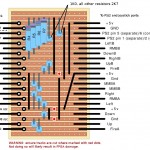
The sprite is currently 16 pixels square, with four bits per pixel in a “1-bit truecolour” arrangement.  Bit 3 indicates opaque/transparent, then bits 2 downto 0 are red, green and blue on/off.  I might change this at some point to a proper paletted arrangement, since that would allow 15 colours (plus transparent) rather than just 8.

The other interesting addition this time round is a simplistic UART.  There are many UARTs available on OpenCores, some of which are very simple and some of which are very full-featured and complicated.  I picked the simplest one I could find, compiled it and saw a Quartus build log full of warnings about latches.  I then decided that since this is a learning exercise, I’d write my own simple UART from scratch.

In the process I did learn one very important lesson, which is that it’s not safe to make a state machine switch states based on an asynchronous signal, such as the rxd line from an RS232 serial port.

The problem is that, while a construct such as

if rxd='0' then
  rxstate<=start;
end if

looks to a programmer’s eye as though it should trigger an atomic operation in response to a low level on rxd, that’s not how it works in practice.  Instead, in an FPGA, leaving one state and entering another can be quite distinct operations, and if they’re triggered by an asynchronous signal that happens to change too close to a clock edge, it’s possible for one to happen without the other!  This leaves the state machine in an illegal state, and usually stalls it.

The solution is very simple – simply delay the rxd signal by one clock, through a register:

if rising_edge(clk)
  rxd_sync <= rxd;
end if;

As simple as that.  rxd_sync is guaranteed to show the same state at a rising clock edge even if sampled through different paths, so using that instead of the raw rxd signal results in working state machines.

[Edit: It’s not actually as simple as that.  When a signal changes too close to a clock edge it can set up an oscillation (metastability) in the target register which can last for an indeterminate amount of time.  It’s possible, though rare, for that amount of time to be longer than a single clock cycle, so to minimise the chances of it causing problems we delay the signal through two synchronisation registers, which effectively squares the tiny probability of a metastable signal wedging the state machine.  It still doesn’t eliminate the problem entirely, but makes it so vanishingly unlikely that unless we’re building something that controls a car, a life-support machine or a spaceship, we can safely ignore it.]

The UART currently runs at 19,200 baud, 1 start bit, 1 stop bit and no parity.  Characters received are echoed to the screen via the character RAM, and also sent back through the UART, so if you use HyperTerminal you’ll see what you’re typing.

The ultimate goal here is to be able to bootstrap the system over the serial port, uploading program code to be executed.  This will avoid having to recompile the entire project every time the code changes.

One other minor change this time round: the master clock frequency has been increased from 100Mhz to 112.5 Mhz.  In the process I’ve added some timing constraints to the SDRAM interface and made a few other tweaks which were necessary to make it stable at that speed.

Full source and binary for anyone who might be interested, available here.

Experimenting with TG68

Part 5 – Interrupts and other tweaks

Since my last post I’ve made a few structural changes to the project, most notably to the video controller.  Rather than just being a collection of ad-hoc lines in the toplevel file, I’ve moved it into a self-contained module and also moved the vgacache out of the SDRAM controller and into this new video_controller module.

As yet another learning exercise, I’ve also added a simple character ROM (character definitions taken from the Minimig boot code), and text buffer, which is merged with the display.  This will no doubt provide a useful debugging display as the project progresses!

The new video_controller module will eventually support a certain amount of runtime adjustment to the video, through some registers exposed to the TG68 processor.  Currently only 1 32-bit register is implemented, which is the framebuffer address.  This means the processor can now scroll the display vertically.

In order to do this smoothly, the framebuffer pointer must be updated during the vertical blanking interval – and the best way to do that is to use a VBLANK interrupt.  Therefore I’ve also created a simple interrupt controller.  This detects momentary pulses on seven different interrupt lines, and encodes them into the 3-bit IPL signal used by the TG68 processor.  I’ve used interrupt level 1 for the VBLANK interrupt, and left the others unused for now.  When I come to add keyboard and mouse support, another interrupt will be used to signal that a byte of PS/2 data is ready.

Binary (.sof file) and full source for anyone who might be interested, can be found here.

Experimenting with TG68

Part 4 – improving memory performance

Since the last instalment I’ve slightly modified the program run by the TG68, so that instead of simply filling a rectangle with the current colour it mixes it with the colour already there.  Quite apart from looking prettier on-screen, this increases the demands on memory access, making for a better testbed for the next stage of the project: caches.

In the current design, when the TG68 wants to access memory, a request signal is raised.  Depending on which part of the SDRAM cycle this happens, it can be up to 15 cycles before the controller notices the request, and if the bus is busy it can be 16 cycles more before the request is serviced.  Since the processor’s waiting around for this to happen, it makes sense to add a temporary buffer into which a pending write can be placed, so the processor can carry on working.  Better yet, since the SDRAM cycle’s already set up for 4-word bursts, if the processor tries to write to an address that will be written during the burst, we can gang the writes up and perform them as one operation.

Likewise, when reading we’re getting four-word bursts from the SDRAM controller, so it makes sense to store all four words, which lets us respond immediately if the processor then asks for another word from the same burst.

There are a couple of complications we have to take care of.  Firstly, when writing the processor uses two signals to indicate which of the high and low bytes of the word should be written.  This allows byte writes even though the bus is 16-bits wide.  The write cache has to store these signals alongside the data to be written.

The other complication, which I haven’t yet attended to, since it doesn’t affect this test project, is that with both read and write caches in use, it’s possible for the read cache to contain stale data.  To fix this, I just need to mark the read cache as dirty if it holds data from an address that’s being written to.

The code, as always, for anyone who might be interested, can be downloaded here.

Experimenting with TG68

Part 3 – Writing to the framebuffer

The previous instalment of this project saw a working VGA framebuffer being filled by an automated hardware process.  Since then I’ve managed to get the TG68 processor running a program from a blockram-based ROM, and writing to the DE1 board’s SDRAM.

The framebuffer being filled by the TG68.

The memory map for the TG68 looks something like this:

  • $000000: ROM (at the moment the ROM code just runs sequentially from $000008.  Will eventually need to put an interrupt table in place and move the code elsewhere.)
  • $0FFFFA: A couple of variables
  • $100000: The frambuffer
  • $7FFFFE: The initial stack pointer

For the ROM I use an M4K blockram, with initial contents specified with an MIF file.  To create the MIF I first assemble the code with Easy68K, then convert the S-Record file it produces to MIF format using srec_cat, like so:

srec_cat in.S68 -o out.mif -mif 16

The ROM program currently backfills the screen, then draws random rectangles in an incrementing colour.  The display is Hi-Colour (5-6-5) bit, which is dithered to fit the DE1’s 4-bit-per-gun output.

The complete project, for anyone who’s interested, can be found here.

Currently the fill-rate is pretty lousy since only a single 16-bit word can be written per slot.  I need to add a writethrough cache of some kind, preferably one capable of merging successive writes to a single burst.

Possible future plans for the project include:

  • CPU cache – separate instruction and data.  Just one burst (64 bit) initially.
  • Writeback cache – to allow (a) the CPU to continue working while a write is in progress, and (b) to gang sequential writes into a single burst write.
    Sprite controller – just one sprite for mouse pointer.
  • Multiple screenmodes.
    •  8bit
    •  lowres
    •  scandoubled?
    •  PAL?
  • Sprite controller.  Just one sprite, for a mouse pointer.
  • A colourtable for indexed modes
  • VBlank interrupt
  • Interrupts in general
  • SD card interface
  • PS/2 controller
  • Hardware registers for framebuffer address, sprite position, PS2 data, etc.
  • Sound

Experimenting with TG68

Part 2: A VGA controller

My first experiments with the TG68 processor didn’t involve RAM at all – it simply ran from a tiny hard-coded ROM and poked an incrementing counter into a hardware register.  In preparation for getting the processor working from RAM I’ve been experimenting with the SDRAM controller from the Minimig Project, and having combined it with the simple VGA timings generator used in the Chameleon Pong core, I now have a working VGA framebuffer

VGA Framebuffer in operation

Not much to look at, I know!

The DE1 Minimig’s SDRAM controller runs on a fixed 16-state cycle, using 4-word bursts, so it can move a maximum of 64 bits per round-trip.  I use the same clock for SDRAM and VGA master clock, and at 640×480 pixels, I need one pixel every 4 clocks.  I’m using 16-bits per pixel (5-6-5 hi-colour), so the display needs 4 words or 64 bits every 16 clocks, which means while data’s being displayed it’s saturating the SDRAM controller.

Luckily there are various tricks we can employ to provide extra bandwidth.  The most obvious one, using a smarter, more dynamic SDRAM controller isn’t actually ideal, because generally speaking the smarter a controller is the less predictable its response time will be.  The other reason I didn’t want to toss out the controller completely and start again is that I wanted to be able to bring any improvement I made to the controller back into the Minimig project.  (The third reason, of course, is that writing a good SDRAM controller is *hard*!)

SDRAM is organised into banks, and the chip used in the DE1 board uses four of them.  These are more-or-less independent, so it’s possible to start a read on one bank while a read to another is still taking place.  This means that it’s possible to add a second time-slot to the SDRAM controller, 180 degrees out of phase with the first.  All I have to do is ensure that I don’t allow the same bank to be accessed from both slots.

I split the RAM up such that adjacent 4-word bursts would come from different banks, like so:

|----------- bank 0 ---------|--------- bank 1 ----------|--------- bank 2 ----------
  word0  word1  word2  word3  word0  word1  word2  word3  word0  word1  word2  word3
 | 0  1 | 2  3 | 4  5 | 6  7 | 8  9 | A  B | C  D | E  F | ...

Because both the reading and writing processes in my design would be accessing memory sequentially, arranging the banks this way should prevent either process being held off for more than one slot.

The other thing I needed to take care of was refresh cycles.  Since both slots need to be held off while a refresh happens, I needed to prevent them happening while data was being displayed, so simply arranged for them to happen at the end of each scanline.

For anyone that’s interested, the demo project can be downloaded here.

There are still  a couple of timing glitches, but if you see them, pressing the reset button (key0) a few times should clear it.  The fill rate isn’t great, but that’s because writes are currently not happening in burst mode, so only one word at a time is written.  This means it takes at least four full frames to write to the entire screen.

The TG68 processor isn’t actually involved in this part of the project – instead there’s a simple hardware process filling the frame.  The next stage will be making the TG68 draw something.


GameSupport music example

Here’s a little demo program written in AMOSPro demonstrating how to use the “GSTrack Loop” commands from the GameSupport extension.  For this demo I used Yannis Brown’s cover of Tequila Slammer, found on Aminet.  When the program starts up, just the first two patterns in the module will play repeatedly, until you press a key, at which point the rest of the song will play.

As the song plays, the demo will report on any “command 8” events reported by the playroutine.  Command 8 is unused in ProTracker, so it’s a useful method of synchronising program events with the music.

Any time you press the space bar, the program will play a “jingle” (the last pattern of the song, in this case), then pick up where it left off.

If anyone finds this interesting or useful, it can be found here:

Download in ADF format

Download in LHA format

Pong revisited

Creating a Pong-style game seems to be a “Hello World” style project for FPGA developers, and was one of the first projects I attempted when I started experimenting with VHDL.

The platform for this project is the truly brilliant Turbo Chameleon 64 cartridge.  For anyone who’s not familiar with this piece of kit, it’s an FPGA device that can be used either as a standalone miniature computer, or as a cartridge attached to a Commodore 64!

Originally designed to provide a VGA output for a Commodore 64, the project’s grown and while it performs that initial task admirably, it has a near flawless emulation of the *entire* C64, provides SD card emulation of disk drives, REU emulation and even freezer cartridge emulation!

It can also run other cores, and has suffiicent flash onboard to store 16 of them.  So far, cores are available to emulate the C64, 48K Spectrum, Amiga (Minimig), and also a neat Game of Life core which makes use of the parallel nature of FPGAs to calculate an entire row of cells at a time.

There’s also a hardware test core, which I used as a starting point for this project.  To try it out, just use the Chameleon’s Chaco program to upload the .rbf file into a free slot, then launch the core from the Chameleon’s own menu.

When it starts up, it will launch into a game between two computer-controlled players.  To take over from one of the players, just click the left mouse button on an attached PS/2 mouse.  A second player can use a mouse attached to the keyboard socket.

The reset button resets the scores, and the menu button exits the Pong core and returns to the Chameleon C64 core.

Click here to download full source and binary.

Experimenting with TG68

Part 1: a counter

The TG68 softcore processor is an MC68000-compatible processor core written by Tobias Gubener, and used in the DE1, DE2 and Turbo Chameleon 64 ports of the Minimig project.  The latest version of the core also supports most 68020 instructions,making it a pretty powerful and useful general purpose processor for FPGA applications.

As a learning exercise I wanted to try using the TG68 in a minimal project – a first step towards the “build-my-own-computer” dream I alluded to in an earlier post.

The TG68 consists of two layers – there’s the processor core itself which has a pretty simple interface, then there’s a wrapper which makes it largely signal-compatible with a “real” 68k processor.  For this project I’ve used the wrapper – but later projects will show how the processor can be used “bare”.

To test the processor, I’ve created a very simple program, assembled with Easy68k.

ORG    $0000
    dc.l      $0      ; Initial Stack Pointer
    dc.l      $8      ; Initial Program Counter
START:                ; first instruction of program
    addq.w    #1,d0
    move.w    d0,$dff180
    bra.s    START

    END    START        ; last line of source

This program runs in a loop which increases register D0 by 1 each iteration, and writes the new value to location $dff180.  (This is the location of the background colour register in the Amiga’s custom chipset – so this program, running on an Amiga, would result in a colourful flickering screen, similar to many decrunchers back in the day.)

The minimal program above assembles to a mere 5 words:

$08: $5240
$0A: $33C0
$0C: $00DF
$0E: $F180
$10: $60F6

(Note that the longword at location 0 is the initial Stack Pointer, and at location 4 is the initial Program Counter, so we start the actual program at location 8.)

In the interests of getting the processor up and running with as little effort at possible, I’ve not attempted to run the program from RAM – instead I decode the appropriate addresses directly in VHDL, like so:

process(clk,cpu_addr)
begin
    if rising_edge(clk) then
        if cpu_as='0' then    -- The CPU has asserted Address Strobe, so decode the address...
            case cpu_addr(23 downto 0) is
                -- We have a simple program encoded into five words here...
                when X"000006" =>
                    cpu_datain <= X"0008"; -- Initial program counter.  Initial stack pointer and high word of PC are zero.
                    cpu_dtack<='0';    
                when X"000008" =>
                    cpu_datain <= X"5240";  -- start: addq.w #1,d0
                    cpu_dtack<='0';    
                when X"00000A" =>
                    cpu_datain <= X"33c0";  -- move.w d0...
                    cpu_dtack<='0';
                when X"00000C" =>
                    cpu_datain <= X"00DF";  -- ...
                    cpu_dtack<='0';    
                when X"00000E" =>
                    cpu_datain <= X"F180";  -- ...,$dff180
                    cpu_dtack<='0';    
                when X"000010" =>
                    cpu_datain <= X"60f6";  -- bra.s start
                    cpu_dtack<='0';

                -- Now a simple hardware register at 0xdff180, written to by the program:
                when X"dff180" =>
                    if cpu_r_w='0' and cpu_uds='0' and cpu_lds='0' then    -- write cycle to the complete word...
                        counter<=cpu_dataout;
                        cpu_dtack<='0';
                    end if;

                -- For any other address we simply return zero.
                when others =>
                    cpu_datain <= X"0000";
                    cpu_dtack<='0';
            end case;
        end if;

        -- When the CPU releases Data Strobe we release dtack.
        -- (No real need to do this, provided everything responds in a single cycle.  DTACK Grounded!)
        if cpu_uds='1' and cpu_lds='1' then
            cpu_dtack<='1';
        end if;
    end if;
end process;

When the processor writes to $dff180, the VHDL snippet above captures the value written, and in the full project writes it to the Hex display on the DE1 board.

The complete Quartus project can be downloaded here if you’re interested.  It runs fast enough that the hex display appears to just read “8888”, but if you press Key0, which acts as a reset button, you can freeze the display and read off the number.  Signaltap can be used to get a better look at what’s going on:

Minimig on the DE1 dev board

In my previous post I talked about FPGAs and the Minimig project.  One of the platforms that has received a port of Minimig is the Altera/Terasic DE1 FPGA development board.  This is a nice little board which comes with a Cyclone 2 FPGA, 8 meg of SDRAM, some SRAM, some flash and a controller chip to configure the FPGA at power-on.  It also has an SD card slot, PS/2 keyboard port, VGA out, an RS232 serial port, an audio codec, some switches, LEDs and a couple of 40-pin general purpose IO headers.

The one downside to this board is that the FPGA is a bit poky, with only about 20,000 logic elements – only just enough to hold the Minimig design, and not large enough to hold the latest 68020 version of the TG68 softcore.

The original DE1 port of Minimig can be found here, while a fork which will hopefully see some new developments in the future can be found here.  Binaries are available, and also complete source if anyone’s else is interested in playing with it.

While the DE1 board has a PS/2 keyboard port, there’s no mouse port and (unsurprisingly!) no DB9 joystick ports – so these need to be added via an extra board connected to one of the GPIO headers.  The source archives contain a suitable schematic, but since my circuit creation skills don’t yet extend beyond stripboard, I made a stripboard layout for the extra board. The layout and a couple of photos of the completed board appear below: