Success!

I found the source of my Minimig-core problems – one was a misrouting of the SD-card’s chip select signal, and the other was interference from the Action Replay module, which isn’t usable with this version of the core anyway, so I’ve simply disabled it.

The core itself now runs very nicely on the C3 board, with the same basic feature set as the Chameleon core:  On top of the normal Minimig feature set, thanks to the efforts of Tobias Gubener it supports 68020-compatible soft processor, and up to 8 meg of Fast RAM.  My own tweaks to the OSD firmware added support for WinUAE-style HDFs and direct SD card access as well as some other minor tweaks.

There are plenty of further tweaks to be made and problems to solve, but after the frustrations of trying to get it working a few days ago, it’s nice to be able to play some Amiga games on it today!

Here’s Syndicate (courtesy of WHDLoad)

And the workbench from my old A4000, running from an SD card partition.

(The original was DblNTSC.  Interesting that PAL Hi Res should look good on a widescreen monitor!)

Full source and bitstream files for the core are available for download here.

So Close!

Here’s my Cyclone III board nearly running the Minimig core.  For it to be getting as far as this error message means it’s correctly loading and running the OSD firmware from the SD card.  I just have some SPI bugs to iron out, but after that I hope it’ll actually run, and then I can figure out how to give the emulated Amiga access to more of the 32 meg of RAM this board contains.

What will be very interesting is to see whether this version suffers from the same build-to-build stability problems that plague the Chameleon port of the core (since hardware-wise it’s almost identical).  Once again, my ultimate goal is to have multiple ports of the core buildable from a single source tree.

Experimenting with TG68

Part 10 – Multiple Boards

Now my A/V and power boards are built and working, I want to run the TG68 MiniSOC project on the Ebay-sourced Cyclone III board.  Rather than just port the project to the new board and then neglect the DE1, what I’ve done this time around is to make a single source tree usable with both the DE1 and C3 boards.

In order to keep things straight, I’ve adopted the following directory structure:

  • RTL – modules belonging to the project itself, and which can be used on either board
  • C3BoardRTL – toplevel and support modules specific to the Cyclone III board
  • C3BoardRTL/Generated – Megafunctions specific to the Cyclone III board, such as the PLL module, BootROM and Character RAM.
  • C3BoardProject – The Quartus project file and the generated .sof / .pof files end up here.
  • DE1RTL – toplevel and support modules specific to the DE1 board.
  • DE1RTL/Generated – PLL, BootROM, CharRAM, etc.
  • DE1Project – The Quartus project file, etc.

At some stage I shall add port the project to the Turbo Chameleon 64, too, and have a third platform buildable from the same source tree.

There are three other noteworthy developments since last time:

Firstly, I finally received the Max3232 chip I was waiting for, so the power board now sports an RS232 serial port, tested and working.

Secondly, as well as receiving an S-record over the serial port, the boot firmware can now load a program (again in S-record format) directly from an SD card.  If you want to try it out, just copy the file CFirmware/out.srec to the root of the SD card, and rename it to “boot.sre”.  As before, you’ll want test.img on the SD card too.

Finally, since my A/V board supports 6-bit per gun video output and the DE1 only supports 4, I’ve moved the dithering out of the vga controller and into a generic module which is instantiated by the board-specific toplevels.  A generic parameter sets the number of available bits per pixel and adjusts the dithering accordingly.

Full source is available, as always, for anyone who might be interested: TG68MiniSOC_Part10_MultiBoard.zip

I also promised in my last post to release the Eagle files for the VGA board once I’d tested the PS/2 sockets, so again, for anyone who might be interested: C3_VGABoard.zip

A custom VGA output board

The Cyclone III board I’m using has a nice roomy EP3C25 FPGA with about 25,000 logic elements and 32 meg of SDRAM, but is rather lacking in ports for talking to the outside world.  I plan to add an RS232 serial port to the power board which featured in my last post, just as soon as I receive the requisite components.

The power board connects to the two least useful of the board’s GPIO headers; most of the IOs on these headers are used up by the SDRAM, but the other two GPIOs are almost fully functional.  (On the EP3C16 version of the board, all 36 IOs on these headers are available – but the EP3C25 needs more power pins, so a few of the IOs are unavailable to me.)

In approximate order of importance, the ports I want to add to this project are:

  • VGA
  • PS/2 keyboard and mouse
  • Audio
  • SD card
  • Joystick (9-pin DSub, Atari/Amiga style)
  • Ethernet – if at all possible.

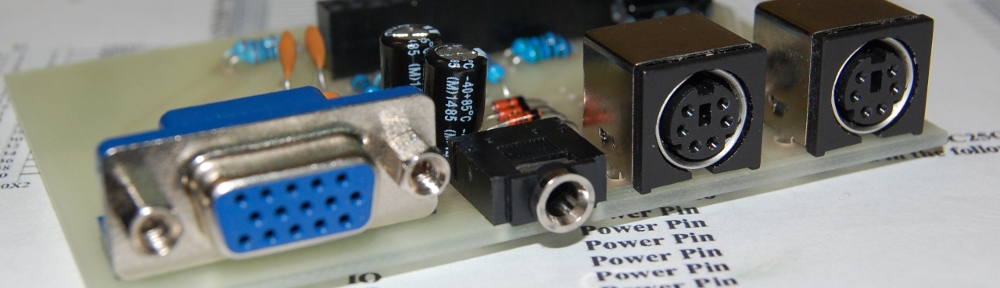
The VGA port requires three individual resistor ladder DACs, which means a fairly high component count, so I wasn’t keen to try building this particular interface on stripboard.  Therefore I decided to try having a custom PCB made.

I used the freeware edition of Eagle to produce the schematic of my board and lay it down, and learned a great deal in the process.  Since including just the VGA port would have been a waste of the remaining pins on the header, I also included the PS/2 ports and audio port on this board (using the DE1 and Minimig schematics as reference).

I made a few mistakes in the process, which I shall avoid next time!  Most importantly, I wasn’t entirely clear about which side of the board was which.  I now know that by default components placed in Eagle are assumed to be on the top layer of the board, with through-hole components being soldered at the back – but I routed the traces on the top layer, intending to treat that as the solder-side and place the components on the other side.  I’d correctly flipped the components to deal with this, but it confused the PCB fab house and delayed things a little.  What I should have done was place everything the right way round, then route the traces onto layer 16 (the back of the board) instead of layer 1.

I used Futurlec to make the PCBs; they seem to be the most affordable option for a hobbyist who only wants a couple of boards.  Because I’d opted for the cheapest shipping method, the boards took a couple of weeks to arrive, but I received them on Friday, and have almost finished populating the first one!

This board attaches to J1 on the FPGA board, and provides a 6-bit resistor ladder for each colour, giving a theoretical 262,144 colours without dithering.

I haven’t yet tested the PS/2 sockets, since I’m waiting for a delivery of the right value of resistor to complete the board – but once it’s verified as working I’ll make the Eagle files available for download.

The 6-bit resistor ladder probably deserves some explanation, since it was an interesting problem to solve.  The VGA specification says that the maximum voltage on the R, G and B pins should be 0.7v, and the load on these pins (i.e. the monitor) should have an impedance of 75 ohms.  The FPGA either drives each pin to +3.3v or to gnd, so the FPGA, the resistor ladder and the load form a complicated potential divider.

Since it’s non-trivial to calculate the voltage produced for an arbitrary input to the resistor ladder, I created a spreadsheet to do the job, and found a combination of standard value resistors that would give a maximum value very close to 0.7v.

The spreadsheet, in case anyone’s interested, can be found here.

The resistor values I settled on were:

  • 525R (formed with a 1K and 1K1 in parallel – which, yes I know, adds a large potential error where you want it least, but also gives you scope to trim that error by swapping resistors in the hope of finding a good match.)
  • 1K1
  • 2K2
  • 4K3
  • 9K1
  • 18K

So does it work?  As always, a picture speaks a thousand words:

As Nature intended!

In my last post I mentioned removing the blue LEDs from the fascia of the case I plan to use for my FPGA project.  I have an extreme dislike of blue LEDs – or at least of the seemingly universal pervasiveness of blue LEDs.  We’ve been able to make them cheaply for, what, a decade now?  Get over it, people!  It’s not novel any more.  They’re annoyingly bright and unpleasantly piercing.  I’m tired of hiding them behind Post-it notes.

So I replaced these obnoxious blue LEDs with bog-standard red, yellow, orange and green LEDs, which worked but weren’t really bright enough to shine through the diffusing layer on the case.  (This layer’s task is presumably to make the blue LEDs vaguely bearable.  Hint: you can make them much *more* bearable by not using them in the first place.)

I ordered some high-brightness LEDs, somewhat skeptical about how different they’d be.  The difference is dramatic, and the LEDs are now clearly visible even in strong light:

There!  Doesn’t that look much nicer than a row of blue lights?

Latching power circuit – in the flesh!

Having breadboarded the latching power circuit from my last post and found it works pretty well, I’ve made a more permanent version that plugs directly onto the headers on my Cyclone 3 board.  While I’d normally build something like this on stripboard, it’s not really appropriate for this project because the pins on the 40-pin headers are only one row of holes apart.  Therefore I’ve used matrix board this time around.

This is the case I plan to use to house this project.  It’s the case from an old, dead Acer Aspire L320 – a nice looking machine that, unfortunately, seems to have insufficient chipset cooling, so tends to die a horrible death.  Dead ones crop up on Ebay fairly frequently, and with a little bit of cleaning up and removing of label residue, they’re an ideal housing for a project like this one.

Behind the power button is a little circuit board with four LEDs (actually only three on mine, but space for a fourth) and the actual power button switch.  I rewired this board slightly – removed the blue LEDs (*please* people, can we get over the blue LED thing now!) and replaced them with green, yellow, orange and red ones.  I also wired the LED anodes in common, to keep the component count down.  The common anode will be fed from 3.3v through a small resitor, then the four LEDs’ cathodes will be tied directly to FPGA pins.  When the respective FPGA pin is low, the LED will light up.

The obvious problem with this arrangement is that when more than one LED is lit, the current will be shared between them, making them dimmer – to avoid this, I’ll use a pulse-width modulation system, giving each LED a 25% duty cycle, and alternating between them, so no two LEDs will be lit at the same time.

The VHDL code for this is as follows:

library ieee;
use ieee.std_logic_1164.all;
use ieee.std_logic_unsigned.all;
use IEEE.numeric_std.ALL;

entity statusleds_pwm is
    port(
        clk : in std_logic;
        leds_in : in std_logic_vector(3 downto 0);
        leds_out : out std_logic_vector(3 downto 0)
    );
end statusleds_pwm;

architecture rtl of statusleds_pwm is
    signal counter : unsigned(18 downto 0);
begin
    process(clk)
    begin
        if rising_edge(clk) then
            counter <= counter+1;
            if counter(16 downto 0)=X"0000"&"0" then
                leds_out<="1111";
                case counter(18 downto 17) is
                    when "00" =>
                        leds_out(0)<=not leds_in(0);
                    when "01" =>
                        leds_out(1)<=not leds_in(1);
                    when "10" =>
                        leds_out(2)<=not leds_in(2);
                    when "11" =>
                        leds_out(3)<=not leds_in(3);
                end case;
            end if;
        end if;
    end process;
end architecture;

As I mentioned in my previous post, the Cyclone 3 board I’m using has four general purpose IO headers, but two of these headers share FPGA pins with the RAM chips, so on a board like mine that’s populated with two RAM chips, there are only a handful of available IOs on headers J3 and J4.  There are, however, enough to run my latching power circuit, the LEDs, and a couple left over which I’ll use for an RS232 port.

The following matrix board layout describes a board which connects directly to headers J3 and J4 on the FPGA board, leaving the IO-rich J1 and J2 free for A/V, SD Card and joystick interfaces.

I’m currently waiting for delivery of some MAX3232s (MAX232 variant that runs from 3.3v) – so that part of the board isn’t yet built – but the power aspect is built and working.

(The above is not quite the final version – I moved one signal to a different IO pin, and added a small capacitor between LED+ and GND.)

Latching power circuit

While the Altera DE1 board has been a great development platform for the MiniSOC project, I don’t want the project to live on that board forever.  I’ve bought a relatively cheap Cyclone 3 board from EBay featuring an EP3C25 FPGA (this is the same FPGA as appears in the Turbo Chameleon 64), which has a shade under 25,000 logic elements to play with.  (The board in question can be found here: http://www.ebay.co.uk/itm/Cyclone-III-FPGA-EP3C25-board-/270910317225  –  that version has only a single 8-bit wide SDRAM chip, but when I contacted the sellers they were extremely helpful, and added a second chip for just $5 extra.)

I have a rather nice small form factor case in which I’d like to install this project, but the case has a PC-style momentary push-button power switch, so I need some kind of latching power circuit.

The requirements for the circuit are:

  • Must draw only negligible power in the “off” state.
  • Must latch reasonably quickly, and not turn off again until the button is released and pressed again.
  • If FPGA signal pins are used, must not allow voltage to reach them in the “off” state.

After studying a few similar circuits on the web, I decided to use a P-channel MOSFET and a BC547, with the base of the latter being driven by the FPGA.

The schematic of my current circuit is as follows:

A few explanatory notes:

  • PWR_BUTTON and PWR_HOLD are signal pins on the FPGA.  The FPGA is powered from VOUT.
  • S1 triggers the MOSFET and allows power to flow to VOUT
  • The FPGA fires up, and as soon as it’s configured, sets PWR_HOLD to a high output, causing the BC547 to keep the MOSFET open.
  • The FPGA sets PWR_BUTTON to an input with weak pullup, allowing it to detect a second press of the button.  D1 prevents +5V reaching the non-5v-tolerant FPGA pin, and also prevents any voltage reaching that pin while the FPGA is off.  R2 prevents the action of the BC547 interfering with the button press detection.
  • R5 is a load resister that just drains away any stray charge that’s left when the circuit powers off.

The button itself has to be debounced in the FPGA.  The easiest way to do this is just to begin a delay any time the button line’s state changes, then sample it a second time when the delay’s elapsed, and compare.

The VHDL looks like this:

signal debounce_counter : unsigned(11 downto 0) := X"fff"; 
signal power_button_deb : std_logic; 
signal power_button_deb1 : std_logic; 
...
-- debounce the power switch 
    process(clk) 
    begin 
        if rising_edge(clk) then 
            if debounce_counter=X"000" then 
                if power_button_deb1='1' and power_button='1' then    -- Is button stable? 
                    power_button_deb<='1'; 
                elsif power_button_deb1='0' and power_button='0' then 
                    power_button_deb<='0'; 
                else -- No? Start a delay... 
                    debounce_counter<=X"FFF"; 
                end if; 
                power_button_deb1 <= power_button; 
            else 
                debounce_counter<=debounce_counter-1; 
            end if; 
        end if; 
    end process;

Experimenting with TG68

Part 9 – Accessing the SD card

A computer’s not much use without a way to load data onto it, so the latest aspect of this project has been getting the SD card slot doing something useful.

SD cards have more than one way of accessing them – they have a “native” protocol, and then an SPI mode.  While the native mode can provide better performance, an SPI host is a built-in feature of many microcontrollers, and documentation is easier to come by.  The Minimig project uses the SD card in SPI mode, and since I’m using that project for reference wherever I’m finding gaps in my own understanding, I’ve used SPI as well!

At one time it was nearly impossible for a hobbyist to obtain official SD card specifications – thankfully the situation is much improved now, and a simplified specification is now available for free download at https://www.sdcard.org/downloads/pls/

Another useful page for reference is this: http://elm-chan.org/docs/mmc/mmc_e.html

One thing that confused me to start with is that to invoke “CMD0” we have to send 0x40 to the SD card, while “CMD1” ends up being 0x41, and so on.  This is because the SD native protocol employs a ‘0’ start bit, then a ‘1’ transmission bit – and these are retained even in SPI mode.

Another peculiarity of SPI is that communication is always bidirectional; the host provides 8 clocks, and eight bits of data are sent in each direction.  This means that in order to read responses from the card, the host must write a dummy byte for each byte it wishes to receive.

For the MiniSOC project, I’ve added some extra hardware registers in the peripheral controller at base 0x810000

0x20: SD
   On read, returns the data received during the previous
   write operation.
   On write, causes the byte written to the low 8 bits to be
   clocked out, and data from the card to be clocked in.
   Note: this is asynchronous, so it's important to check that any
   previous write has finished!

0x22 SD_CS
  Read: bit 15 indicates whether the SPI host is busy performing
   a transfer
   Write: bit 0 sets the chip select line of the SD card.

0x24 - SD_Blocking.
   This is equivalent to 0x20 except that both reads and writes will
   incur wait states until any previous transfer has completed,
   eliminating the need to poll 0x22.

0x100 onwards:
   This area is deliberately incompletely decoded, so reads from
   anywhere within the region will have the same effect.  Unlike both
   0x20 and 0x24, reading from these registers will trigger a new
   transfer, sending sixteen bits of 0xffff and receiving 16 bits back
   from the SD card.  The point of this is to allow driver code to use
   constructs like this:

; set up a block read command, then...
  lea 0x810100,a0
  lea sector_buffer,a1
  move.l #15,d7
  move.w (a0),d0 ; pump the first 16 bits.
.loop
  movem.l (a0),d0-6/a2 ; pump 64 bits in one command!
  movem.l d0-6/a2,(a1)
  add.l #32,a1
  dbf d7,.loop

This is much faster than receiving data a single byte at a time.

Full source and binaries can be found here, for anyone that might be interested.

To try this out, you’ll need (a) an Altera DE1 board, (b) HyperTerminal or (preferably) something similar but faster, and (c) an SD card containing the file “Test.img” from the Misc directory in the archive.

Use Quartus to program the DE1 with the .sof file.

Use HyperTerminal or similar at 115200 baud, 8N1, to send the file “out.srec” from the CFirmware directory in the archive.  If everything goes to plan, the MiniSOC should load the image, display it on screen, then scroll up and down as before.

One of the next tasks will be to bootstrap directly from the SD card, eliminating the need for serial bootstrapping.

Experimenting with TG68

Part 8 – Timers and C code

Having successfully uploaded an S-record program over RS232 last time, I’ve since followed the helpful instructions in Christian Vogelgsang’s Chameleon Minimig repo for setting up a cross-compilation toolchain.  I’m now able to build C software for this project, which in the absence of a more imaginative name, I’m coming to think of as “MiniSOC”.

(In fact, I haven’t used newlib – and nor did Christian in the finish – instead we’ve drawn from klibc, just cherry-picking the routines needed for the task at hand.  There are also a couple of other dependencies for building GCC – gmp, mpfr and mpc, which are a stack of libraries for handling multi-precision arithmetic.)

Since I’m not familiar with the syntax used by GCC’s assembler (which is very unlike the “normal” Motorola syntax) I also used VASM to build assembly components to Elf format, then the cross-compiled objdump to create S-records from the final project.

I also used srec_cat, as before, to create .mif files from the lowest-level startup file, which ends up in an M4K.

The biggest change hardware-wise this time round is the addition of some timers.  There are now eight in total, two of which directly divide the system clock, and the other six divide the output of the first timer.  Three of those run in continuous mode, and three run as one-shot timers.

An event on any of those six timers will trigger an interrupt, and the one timer I haven’t yet mentioned will eventually be used to provide an SPI clock when I implement SD card access.

The firmware file CFirmware/out.srec contains basically the same graphics demo as previous builds, implemented in assembler, but with the housekeeping and keyboard/mouse drivers in C.  One of the one-shot timers is used to provide a mouse time-out, so the project will still run even if there’s no mouse connected.

Thanks to code borrowed from klibc, the FrameBuffer’s address is no longer hardcoded, and instead is malloc()ed.  Since there’s no operating system to provide memory blocks to the malloc arena, I’ve added a routine to add a hardcoded block of memory for use by malloc().  The actual bounds of that block are specified by the GCC linker script.  This allows me to hardcode the upper bound to match the hardware, but have the lower bound automatically set immediately above the region occupied by the firmware itself.

This version has a keyboard driver, too – incomplete but functional enough that what you type ends up on screen.  Mouse buttons are also detected, and will cause the colours to cycle more rapidly.

Full source and binaries can be found here.

Baby steps towards AGA support

The current publicly available sources for the Minimig project only support the ECS chipset, there’s not yet any support for AGA.  (The Minimig core used by the FPGA Replay board *does*, apparently, have robust AGA support, but the sources haven’t yet been released to the wider world.)

So I decided to have a go at adding a little AGA functionality myself.

Compared with the ECS chipset, the AGA chipset doesn’t actually add that much complexity.  The extra features are basically:

  • Colourtable extended from 32 entries to 256.  There are still only 32 colourtable registers, and they’re accessed in banks, which are selected in another register.
  • Colourtable entries are now 24-bit deep rather than just 12.  A select bit in another register determines whether colourtable writes go to the most- or least-significant 12 bits.
  • There are now 8 bitplanes instead of 6
  • Bitplane data can be exclusive-ored with a mask value.  This enables some neat tricks with “copper chunky” modes, among other things.
  • Sprites can be high-res
  • Data can now be fetched 32-bits at a time, double-pumped or both, giving an effective 64-bit datapath.

The easiest place to start is the colourtables, which in the present Minimig design are stored in registers.  Since the colourtable was about to balloon from 32 12-bit entries to 256 24-bit entries, I migrated the colourtable to a pair of M4Ks – one to take the upper 12-bits of each colour, the other to take the lower 12-bits.

I also implemented enough of the BPLCON3 and BPLCON4 registers to support colourtable bank selection and masking.

I’ve also created a small Copperlist demo in ADF format for testing, which can be found here.

This demo simply uses lower-bit entries and palette masking as a test – the following screenshot shows how it looks under ECS and under AGA.

(Note that while the colourtable entries store 24-bits, they’re still only displayed as 12-bit, because that’s all the DE1 Board’s VGA output can handle without extra dithering, which will come later.)

A git repo containing the current code is here, while a binary can be found here.

Please note that this is highly experimental – there are timing inaccuracies compared with the real chipset, extra-half-brite mode is currently broken. (and the normal Minimig boot text is missing as a result of another experiment to reduce the size of the boot ROM!)