Reading a Sega 6-button pad

Part 2: some code

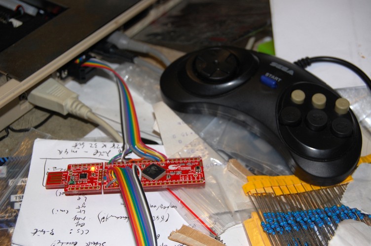
In my earlier post I mentioned that I was going to handle reading the Sega 6-button joypad in software, using an interrupt routine, and use programmable logic to handle masquerading as a CD32 pad.

The six inputs from the Sega pad (up, down, left, right, button1, button2) are mapped to PSOC pins P2.0 to P2.5.  Since these are adjacent, we can read and write to them easily as a single entity.  We create a “pins” component with six inputs, named Sega_Inputs, and PSOC creator automatically generate headers and stubs so that we can read their status in main.c simply by calling Sega_Inputs_Read().  Similarly, we create an output pin, Sega_Select on pin P2.6, which we can write in the code using Sega_Select_Write().

Continue reading

Reading a Sega 6-button pad

Part 1: The Plan

One of the projects I have in mind for the PSOC4 chip on the CY8CKIT-049-42xx boards I picked up recently is an adapter to allow 6-button Sega Megadrive controllers to be used on the Amiga.  I already made such a device a couple of years ago using a PIC microcontroller but never finished the project (I discovered FPGAs round about then!) and the programmable digital blocks in the PSOC4 make it an ideal platform for resurrecting the project.

Initially I shall read the Sega pad in software, using an interrupt routine, then implement the CD32-pad shift register using the programmable hardware in the PSOC4.

The original Sega Megadrive gamepad had four buttons: A, B, C and Start.  The pad used a standard Atari-style 9-pin DSUB connector, and while the four directions and button B were mapped using standard Atari wiring (pins 1,2,3,4,6), button C appeared on pin 9.  Most Atari-like gameport connectors have +5v available on pin 7, but the Sega variant has +5v on pin 5.  Instead, pin 7 is used as a select signal, which multiplexes the pins normally occupied by the B and C buttons.  When the select signal is high, B & C are readable, and when the select signal is low, the status of buttons A and Start appear on those lines instead.

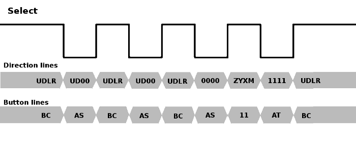
When it came to adding extra buttons to the six button pad, Sega needed to find a way of multiplexing extra buttons in such a way that they didn’t cause compatibility issues.  The obvious solution of making extra buttons replace the direction lines when the select signal is low wasn’t possible because the existing 3-button protocol already held the left and right lines low when select was low, presumably so software could distinguish the 3-button pad from a standard Atari-style joystick or Master System controller.  Instead they went with a “magic knock” approach, in which software toggles the select line four times in quick succession.  The new buttons appear on the directions during the high pulse following the third low pulse, and to identify the pad as a six button button, the direction lines are low and high for the low pulses before and after this, respectively.

SegaPad

Configuring ZPUFlex

In the few months since I started playing around with the zpu_small core, expanding it into what ultimately became ZPUFlex, my variant of the CPU has gone from being an interesting experiment to something that might actually see some usefulness in other projects.

ZPUFlex was intended from the outset to be configurable and flexible, but this comes at the cost of complexity, and there are a number of competing factors to consider when configuring the CPU.  The following is an attempt to document some of the choices that must be made when using ZPUFlex.

Continue reading

PSOC4 – another distraction!

I have a new toy to distract me from my existing projects!

I recently came across this neat little prototyping kit from Cypress Semiconductor, and several aspects of the device piqued my interest:

  • The cost is low enough that you don’t have to think twice about using one in a project
  • The chip has an ARM Cortex M0 CPU core
  • The 42xx version (as opposed to the 41xx version) has a small amount of FPGA-like programmable logic built in
  • The device is programmed via an onboard USB/TTL converter, which in a piece of superbly elegant design can be “snapped off” the board once programming is complete.
  • The device is capable of running from 5v, and handling 5v signals. Continue reading

Experimenting with TG68

Part 14: Improving the SDRAM controller

One limitation of the MiniSOC project so far has been that only a very basic 16-bit 640×480@60Hz screenmode is supported.  The reason for this is mainly RAM bandwidth, since the boards I’m targetting have single-data-rate SDRAM.

The SDRAM controller I’m using is derived from the one Tobias Gubener created for the TG68-based versions of the Minimig core.  The original controller used 4-word bursts when reading from SDRAM, wrote in single words, and operated on a fixed 16-clock cycle, which had the advantage of guaranteeing a deterministic response time for the Amiga emulation. Continue reading

Gotek Floppy Emulator Revisited

The circuit I cobbled together a few weeks ago to add sound support to the Gotek floppy emulator worked up to a point, but it was ugly as hell, and suffered from occasional stray oscillations.  H.M. – the mastermind behind the new Amiga-compatible firmware for the Gotek unit – suggested using a MOSFET instead of the BJTs, and since I’m still shaky on the use of transistors it seemed like a good opportunity to learn.

Continue reading

Experimenting with TG68

Part 13: Timing closure at last!

In the TG68MiniSOC project, I took the lead from the way the CPU was implemented in the Minimig project and clocked everything at a single high-speed clock.

The TG68 itself can’t run at much more than 32MHz, and it it’s only possible to clock it faster than this because it has a “clkena” signal, which allows it to be halted while the combinational logic inside catches up.  While this approach works (mostly) it causes issues for the FPGA synthesis software, which reports severe timing violations when combinational paths are more than a single cycle long.  It’s possible to inform the software that these long paths are OK, and anticipated in the design by way of “multicycles”, but finding and specifying them all, without including anything that shouldn’t be included, is long-winded, tedious and error-prone.  This issue is the primary cause of the build-to-build stability problems that have dogged several TG68-based projects.

Today, however, I’ve been trying a different approach, with split clocks.  This version of the project uses a 100MHz clock for the SDRAM controller and VGA controller, and a 25MHz clock (generated within the same PLL as the 100MHz clock, and thus aligned with it) that runs the CPU, the main state machine and peripherals.  Dealing with data transfer between these two clocks turned out to be much easier than I’d anticipated, and simply making sure that all signals from the CPU are registered before being handed over to anything running at the faster clock rate seems to be the main trick.

The big news is that this approach allows the project to achieve timing closure!  When building for the venerable DE1, TimeQuest no longer reports any timing violations.  I have yet to run any benchmarks on this version of the project, so I don’t yet know what sort of speed penalty the project will suffer, but the increased tidiness of the main state machine, and the added reliability that should come from the tools being able to understand the project’s structure should make the performance penalty well worthwhile.

As always, full source can be found on my github page.  I tag the repository at key points, and this post refers to the code tagged as SplitClock_20140405.

Gotek Floppy Drive emulator

There are various devices on the market which can emulate a floppy drive using disk images on a flash device of some kind.  The best known of these is probably the HxC Floppy Emulator but there’s also a cheaper product, the Gotek floppy emulator.

Until recently the Gotek was no use with the Amiga, since it couldn’t cope with the Amiga’s unusual encoding scheme – all that changed a few weeks ago, however, when Hervé Messinger released a new firmware for the Gotek unit, written from scratch, which provides robust support for Amiga ADF images.

Needless to say, I couldn’t resist buying one of these to play with, and while the flashing process is a bit finicky, once it’s done the drive works well.  I did find the complete silence from the drive a little disconcerting, however, so set out to modify the drive to provide some kind of audible feedback.  Here’s the result:

I did this simply by wiring a couple of transistors to the “Step” signal on the floppy interface, which trigger a piezo sounder.

There are a couple of subtleties to take care of:

In my first attempt I placed the sounder between +12v and the collector of a transistor.  This doesn’t work because a piezo sounder has a very high impedance and appears to the rest of the circuit like a small capacitor.  Thus, when the transistor is activated, the sounder charges, but when the transistor deactivates the sounder is effectively open circuit, so nothing happens to the charge stored within.  Instead, the transistor needs to be in parallel with the sounder, so that it discharges the charge stored in the sounder when activated, and allows fresh charge to build up when deactivated.

The other problem is that the step signal on the floppy interface is a very brief low pulse, with a specified minimum width of 1µs.  In practice it’s quite a bit wider than that, but still very brief compared with the storage time of a typical bipolar junction transistor.  What this means is that the transistor triggered by the Step pulse has to be a fast switching type with a very low storage time.

ProjectXG Revisitied

[This is a post I made to AmiBay back in 2011.  The domain on which I hosted the images and audio snippets is about to expire, so I’ve rescued the files and moved them here – so I may as well archive the post itself too, while I’m at it!]

Anyone remember CU Amiga Magazine’s ProjectXG feature many years ago? They published a parts list and instructions in the magazine for interfacing a Yamaha DB50XG WaveBlaster MIDI daughterboard, intended for use with a PC soundcard, to an Amiga.

Continue reading

Bringing up a new board

Part 1: The Plan!

Having received the ESM-BB10 Spartan 6 board a couple of weeks ago I was naturally keen to see it in action.  Since I only have the free “WebPack” version of Xilinx’s ISE design suite, I can’t use the ChipScope logic analyzer (roughly equivalent to SignalTap, I believe) – so debugging is going to be tricky.  Therefore I’ve taken a methodical, step-by-step approach, testing the various parts of the board one by one.

The ZPUDemos collection is ideal for this purpose, since the projects there range in complexity from a simple “Hello World” that requires no peripherals apart from RS232 serial, to projects that make use of VGA, SDRAM and SD card. Continue reading