OneChipMSX in Chameleon’s Clothing?

Part 1: This should be easy, right?

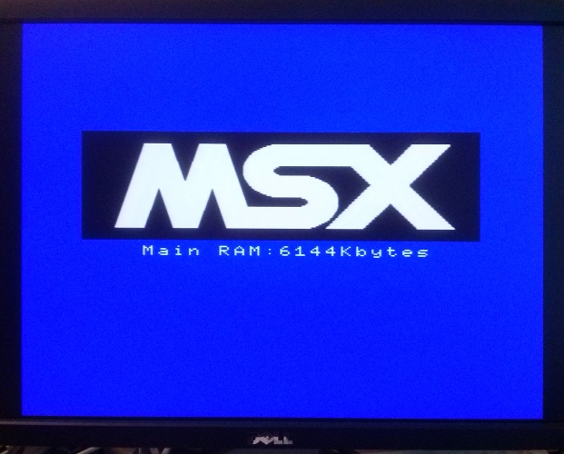
Some months back I was introduced to OneChipMSX by a keen user of the Turbo Chameleon 64 and various other FPGA boards, in the hope that I’d be able to port the project to the Chameleon.

At the time it was a more complicated proposition than I was capable of tackling, but I’ve learned a great deal since then, so recently decided to look again. Continue reading

How many angels…

… can dance on the head of a pin?

I have no idea – but I do know how many ZPUFlex processors will fit in a DE1 dev board: 25!  [Edit: I’ve since managed to squeeze in another one – so 26!]

OK, I’m stretching things a little to claim that 25 fully-featured ZPUFlex CPUs will fit on the DE1, because these have a really tiny ROM and very minimal supporting logic, so Quartus can optimise the hell out of the design – but it still seemed like a fun demo.

Source, as always, can be found on GitHub.

[EDIT: The M4K memory blocks on the DE1’s Cyclone II support 32-bit data width, but not in full dual-port mode, where the data width is limited to 16-bit.  This means that no matter how small the ZPU’s ROM/StackRAM, it will occupy a minimum of 2 M4Ks.  If it weren’t for this fact, I think the DE1 could take 3 further ZPUs.  As it is, it’s possible to add just one more instance of the ZPU, and the code on github now reflects this.  The record for the maxmium number of soft CPUs in a single project on the DE1 board is now 26.  Unless you know diffferent!]

Hello World in 546 Logic Elements!

I wrote once before about the HelloWorld example in my ZPUDemos repository.  This demo used the ZPU processor and a minimal UART to send the archetypal “Hello World!” message to the serial port, and used just 684 logic elements to do so.

I’ve revisited the project, and added a new demo to ZPUDemos, which shows how the ZPU’s size can be reduced even further.

By bringing a copy of the zpu_config.vhd file into the local project directory and modifying some of the constants within we can reduce the size of the CPU’s internal address registers.  This saves quite some logic, since any unused address bits can’t be automatically optimised out, thanks to the fact that addresses can be written to and from the Stack RAM.

Since the HelloWorld ROM is between 1 and 2kb in size we need to use 11 address bits (10 downto 0), and allow one extra bit to produce some IO space, so we set maxAddrBitIncIO to 11.  Since we’re using the de-facto ZPU convention of allowing the MSB to designate IO space, then any operations that don’t involve IO can use a max bit of 10 – thus we leave maxAddrBit set to maxAddrBitIncIO-1.

This change brings the size of the ZPU itself from 549 to 462 logic elements.  This combined with adjusting the peripheral code to deal with the narrower address space, and disabling the UART RX brings the entire HelloWorld project from 692 logic elements (there have been tweaks and bug fixes since the previous result of 684 was achieved) down to 546!

Besides logic area, there is another benefit to trimming unused address logic: simplifying the logic – especially of the 32-bit adder which increments the program counter – relaxes the CPU’s timing requirements somewhat, and there’s a noticeable improvement in fmax as the address space narrows.

Reading a Sega 6-button pad

Part 4: Up and running

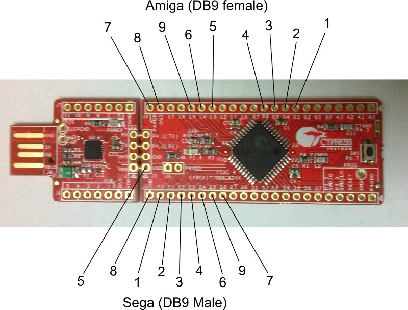
I’m pleased to report that the first prototype of the PSOC4-based Sega 6-button pad to Amiga CD32 adapter is now up and running.  In the process I’ve learned a lot about the PSOC4 platform, and I have to say as a development platform I really like it – I have no doubt I shall be using these devices in future projects.

PSOC Creator Project files for the adapter can be found at https://github.com/robinsonb5/SegaToCD32

Reading a Sega 6-button pad

Part 2: some code

In my earlier post I mentioned that I was going to handle reading the Sega 6-button joypad in software, using an interrupt routine, and use programmable logic to handle masquerading as a CD32 pad.

The six inputs from the Sega pad (up, down, left, right, button1, button2) are mapped to PSOC pins P2.0 to P2.5.  Since these are adjacent, we can read and write to them easily as a single entity.  We create a “pins” component with six inputs, named Sega_Inputs, and PSOC creator automatically generate headers and stubs so that we can read their status in main.c simply by calling Sega_Inputs_Read().  Similarly, we create an output pin, Sega_Select on pin P2.6, which we can write in the code using Sega_Select_Write().

Continue reading