Experimenting with TG68

Part 14: Improving the SDRAM controller

One limitation of the MiniSOC project so far has been that only a very basic 16-bit 640×480@60Hz screenmode is supported.  The reason for this is mainly RAM bandwidth, since the boards I’m targetting have single-data-rate SDRAM.

The SDRAM controller I’m using is derived from the one Tobias Gubener created for the TG68-based versions of the Minimig core.  The original controller used 4-word bursts when reading from SDRAM, wrote in single words, and operated on a fixed 16-clock cycle, which had the advantage of guaranteeing a deterministic response time for the Amiga emulation. Continue reading

Experimenting with TG68

Part 13: Timing closure at last!

In the TG68MiniSOC project, I took the lead from the way the CPU was implemented in the Minimig project and clocked everything at a single high-speed clock.

The TG68 itself can’t run at much more than 32MHz, and it it’s only possible to clock it faster than this because it has a “clkena” signal, which allows it to be halted while the combinational logic inside catches up.  While this approach works (mostly) it causes issues for the FPGA synthesis software, which reports severe timing violations when combinational paths are more than a single cycle long.  It’s possible to inform the software that these long paths are OK, and anticipated in the design by way of “multicycles”, but finding and specifying them all, without including anything that shouldn’t be included, is long-winded, tedious and error-prone.  This issue is the primary cause of the build-to-build stability problems that have dogged several TG68-based projects.

Today, however, I’ve been trying a different approach, with split clocks.  This version of the project uses a 100MHz clock for the SDRAM controller and VGA controller, and a 25MHz clock (generated within the same PLL as the 100MHz clock, and thus aligned with it) that runs the CPU, the main state machine and peripherals.  Dealing with data transfer between these two clocks turned out to be much easier than I’d anticipated, and simply making sure that all signals from the CPU are registered before being handed over to anything running at the faster clock rate seems to be the main trick.

The big news is that this approach allows the project to achieve timing closure!  When building for the venerable DE1, TimeQuest no longer reports any timing violations.  I have yet to run any benchmarks on this version of the project, so I don’t yet know what sort of speed penalty the project will suffer, but the increased tidiness of the main state machine, and the added reliability that should come from the tools being able to understand the project’s structure should make the performance penalty well worthwhile.

As always, full source can be found on my github page.  I tag the repository at key points, and this post refers to the code tagged as SplitClock_20140405.

Bringing up a new board

Part 3: Clocking

The EMS11-BB21 board I received a few weeks ago has a Spartan 6 FPGA which the board provides with a 50MHz clock.  In the examples so far I’ve used that clock directly – but FPGAs generally have the ability to be much more flexible where clocking’s concerned, and the Spartan 6 is no exception. Continue reading

Bringing up a new board

Part 2: Hello World

Since my last post I’ve received yet another board from Emanuel – another prototype FPGA board with Spartan 6, SDRAM and SSRAM.  This one’s a little simpler than the previous board, with no ports other than USB on the board itself, and a daughter card with a VGA connector on it.  Unlike the previous board, which had a 2-bits-per-gun resistor ladder DAC, this one has an ADV7123 video DAC chip – the same one used on the DE2 board – which has an impressive 10 bits per gun.  That’s good enough to do 24-bit true colour with headroom for calibration tables!

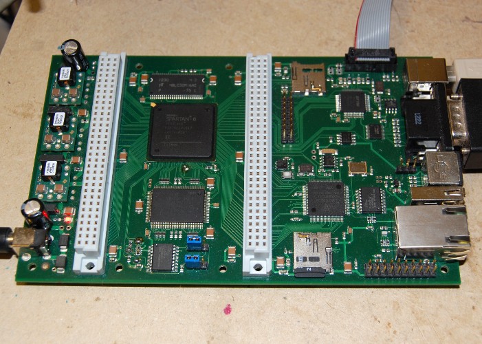
EMS11-BB21

So, let’s get “Hello World” running on this board. Continue reading

Bringing up a new board

Part 1: The Plan!

Having received the ESM-BB10 Spartan 6 board a couple of weeks ago I was naturally keen to see it in action.  Since I only have the free “WebPack” version of Xilinx’s ISE design suite, I can’t use the ChipScope logic analyzer (roughly equivalent to SignalTap, I believe) – so debugging is going to be tricky.  Therefore I’ve taken a methodical, step-by-step approach, testing the various parts of the board one by one.

The ZPUDemos collection is ideal for this purpose, since the projects there range in complexity from a simple “Hello World” that requires no peripherals apart from RS232 serial, to projects that make use of VGA, SDRAM and SD card. Continue reading

No, I haven’t vanished!

Apologies for the lack of recent updates.  I haven’t been completely idle but my time’s being filled with other things at the moment, including replacing light fittings, hanging pictures and learning the guitar!

Despite the silence, I’ve not been completely inactive on the FPGA front, however, and I’m still slowly building my library of demo projects for my “Flex” variant of the ZPU processor.  In the process I’m redesigning and streamlining a lot of the components that made up the TG68MiniSOC project, so that will be updated with the results before too much longer, and I’ve also started branching out from being purely Altera-based into Xilinx too.

This last development is the result of reader Emanuel Stiebler very generously supplying me with a Spartan-6 board!

ESM-BB10

This has an XC6SLX45 FPGA, 32 megabytes of SDRAM, 4 megabyte of SSRAM, a microcontroller, dual micro-SD slots (one for the µC, one for the FPGA) and an assortment of IO ports.

I’ve already ported a few of the ZPU Demos to this new board (and a couple of the simpler ones to the original Minimig board while I’m at it!) but will post about the process in more detail soon.

A Clockport for the Chameleon64’s Minimig?

Christian Vogelgsang, who a couple of years ago collected together the git repository of Tobias Gubener’s Minimig_tc64 project and ported the OSD menu code to GCC – thus sparking my interesting and subsequent foray into the world of FPGA development – has been hard at work once again!  This time he’s succeeded in adding support for the Chameleon’s clockport to the Minimig core, which means that in theory a good proportion of clockport peripherals should now be usable!

So far it’s only been tested with a Silver Surfer card – it will be most interesting to see which cards work without any further changes, and which prove to be troublesome.

Links to source, binary and details of a small hardware hack required can be found on Chris’s blog – but before downloading and trying them take note that

THIS MUST NOT BE USED WHILE THE CARTRIDGE IS PLUGGED INTO A C64.

The IO mux code has been stripped right down to bare bones to give usable clockport performance, and the synchronization with C64 bus cycles is no longer present, so a connected C64 will definitely crash, and may even be damaged.

With that warning in mind, do check out his work here: http://lallafa.de/blog/2013/09/a-clockport-for-chameleon64s-minimig/

Hello World in 684 logic elements!

You may have noticed the new “ZPU” section on the header of this site. The ZPU is a very useful little processor, and I think it’s under-appreciated because of a lack of documentation and design examples – so I’m trying to redress the balance a bit with my ZPUDemos repository.

So far I have a very simple Hello World project, which on an Altera DE1 board takes up a tiny 684 logic elements, including RS232 transmission. The ROM is also pretty tiny, bearing in mind it’s written in C, at under 2kb.

The repo also now contains Dhrystone benchmark projects, which use the ZPUFlex variant both with and without the optional hardware instructions, turning in about 1.7 DMIPS for the barebones configuration, and 5.1 DMIPS for the version with optional hardware instructions enabled.

More demos will follow in due course.

Learn something new every day…

So while I’m experimenting with FPGA boards I generally upload a design into them at runtime via a USB-Blaster JTAG cable, and only rarely do I store a design permanently in a board’s configuration device.

Some of the boards I use have two separate connectors for the USB Blaster – one for direct programming of the FPGA and the other for Active Serial programming of an EPCS series flash device.  Others have an onboard microcontroller which handle configuration – and then there’s the Vampire 500 board.  This has a single JTAG connector and an EPCS4 configuration device, but no immediately obvious means of programming the EPCS4. Continue reading